The High-Electron Mobility Transistor at 30: I mpressive - PowerPoint PPT Presentation
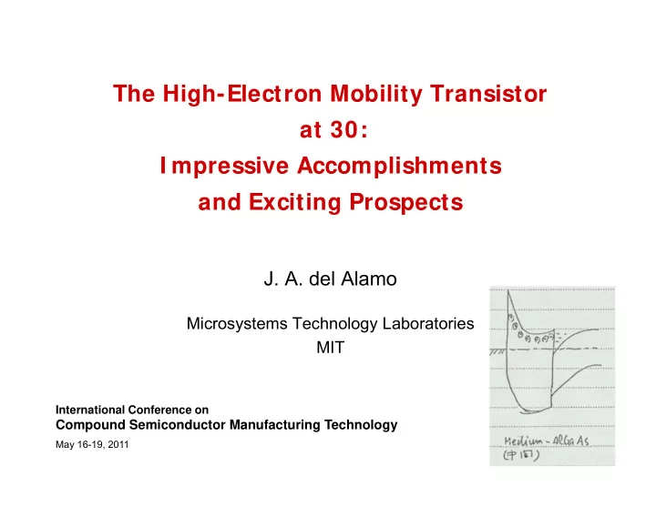
The High-Electron Mobility Transistor at 30: I mpressive Accomplishments and Exciting Prospects J. A. del Alamo Microsystems Technology Laboratories MIT International Conference on Compound Semiconductor Manufacturing Technology May 16-19,
The High-Electron Mobility Transistor at 30: I mpressive Accomplishments and Exciting Prospects J. A. del Alamo Microsystems Technology Laboratories MIT International Conference on Compound Semiconductor Manufacturing Technology May 16-19, 2011
Outline • Introduction • HEMT electronics • Modulation-doped structures in physics • Future prospects 2
The High Electron Mobility Transistor Mimura, JJAPL 1980 3
Energy band diagrams in Mimura’s patent application (Aug. 16, 1979) Courtesy of Takashi Mimura (Fujitsu) 4
Modulation doping • High electron mobility in modulation-doped AlGaAs/GaAs heterostructures • 2 DEG at AlGaAs/GaAs interface Enhanced Dingle, APL 1978 Störmer, Solid St Comm 1979 5
HEMT by other name… U. Illinois: Thomson-CSF: Bell Labs.: Modulation-Doped FET Two-Dimensional Electron Selectively-Doped (MODFET) Gas FET (TEGFET) Heterojunction Transistor (SDHT) Laviron, EL 1981 Su, EL 1982 DiLorenzo, IEDM 1982 6
And the winner is… # papers in Compendex and Inspec databases with keyword in title, abstract or indexing terms Data courtesy of Angie Locknar (MIT Libraries) 7
First HEMT I C 27-stage ring oscillator E/D logic “The switching delay of 17.1 ps is the lowest of all the semiconductor logic technologies reported thus far.” Mimura, JJAPL 1981 “HEMT technology is presenting new possibilities for high- speed low-power very-large-scale-integration.” 8
HEMT I Cs ride Moore’s Law 1 Kb SRAM 16 Kb SRAM 64 Kb SRAM 1984: 1 Kb SRAM (7,244 HEMTs, 8.7 mm 2 ) 1984: 4 Kb SRAM (26,864 HEMTs, 21 mm 2 ) 1987: 16 Kb SRAM (107,519 HEMTs, 24 mm 2 ) 1991: 64 Kb SRAM (>462,000 HEMTs, 48 mm 2 ) Abe, JSSC 1991 Watanabe, TED 1987 Abe, JVST1987 Suzuki, JSSC 1991 9
First HEMT LNA 20 GHz 4-stage HEMT LNA (1983) Niori, ISSCC 1983 Great improvement in noise characteristics as T ↓ 10
Early commercial applications First commercial HEMT product: First mass market product: 0.25 μ m cryogenic low-noise amplifier at GaAs HEMTs for LNA in DBS Nobeyama Radio Observatory receiver (1987) (1985) 12 GHz Mimura, Surf Sci 1990 Mimura, JJAP 2005 Used to discover new interstellar By 1988, world wide production of molecule C 6 H in Taurus HEMT receivers reached 20 Molecular Cloud (1986) million/year 11
Delta-doped pseudomorphic HEMT Delta doping Pseudomorphic HEMT Ketterson, EDL 1985 Chao, IEDM 1987 • Motivation: lower x in Al x Ga 1-x As • Enabled barrier thickness scaling to avoid carrier freeze-out improved transconductance • Enhanced transport in InGaAs and scalability • Large ∆ E c enhanced current • Enhancement of breakdown voltage 12
PHEMT I Cs UMTS-LTE PA module Chow, MTT-S 2008 77 GHz transceiver 40 Gb/s modulator driver Tessmann, GaAs IC Carroll, MTT-S 2002 1999 Bipolar/E-D PHEMT process Henderson, Mantech 2007 Single-chip WLAN MMIC, Morkner, RFIC 2007 Single MOCVD growth 13
HEMT markets 2009 HEMT MMIC $1.2B expected market segmentation in 2011 (Total=$944 M) • Biggest market: wireless communications • Biggest applications: cell phone handsets, WLAN, base stations and CATV Data courtesy of Eric Higham (Strategy Analytics) 14
HEMTs in other material systems InAlAs/InGaAs on InP SiGe/Si AlGaN/GaN Daembkes, TED 1986 Khan, APL 1993 Chen, EDL 1982 Also: AlSb/InAs, AlInSb/InSb, etc 15
High Hole Mobility Transistors AlGaAs/GaAs Si/SiGe AlSbAs/GaSb Pearsall, EDL 1986 Luo, EDL 1990 Störmer, APL 1984 Also: AlGaAs/InGaAs, InAlAs/InGaAs, AlGaSb/InGaSb, InGaN/GaN, etc 16
Complementary HEMT/ HHMT I Cs AlGaAs/GaAs system Cirillo, IEDM 1985 171,000 transistor 16- channel signal distribution system Also: InAlAs/InGaAs system Brown, Trans VLSI Syst 1998 17
I nAlAs/ I nGaAs HEMTs on I nP Uniqueness: very high mobility and velocity record frequency response at very low voltage f max =1.25 THz @ 0.8 V 300 600 700 = f avg = f f 1500 m ax Kim, IEDM 2010 This work 1000 f max [GHz] f T =644 GHz, f max =681 GHz @ 0.5 V Kim, EDL 2010 MIT HEMT Fujitsu HEMT NGAS HEMT 500 SNU HEMT UCSB HBT UIUC HBT Postech HBT HRL HBT ETH HBT 5-stage 480 GHz amp (G=11.7 dB) 0 0 500 1000 f T [GHz] Deal, MWCL 2010 18
I nAlAs/ I nGaAs HEMT mmw I Cs 120-GHz-band link at Beijing Olympics (10 Gb/s over 1 km) RX, TX, PA single-chip modules: JC Fuji TV booth 0.1 μm InP HEMT Live-uncompressed HD video Water Cube National Stadium TV station (Japan) Hirata, TMTT 2009 Courtesy of Akihiko Hirata (NTT) 19
I nAlAs/ I nGaAs Metamorphic HEMTs on GaAs LNA NF vs. f Wang, TED 1988 80 Gb/s multiplexer IC Wurfl, GAAS 2004 Tessmann, CSIC 2010 Single-stage 500 GHz LNA (G=3.3 dB) • Comparable performance to InP substrate • Improved manufacturability • Lower cost • Well established packaging technology LNA data courtesy of Phillip Smith (BAE Systems) 20
Polarization doping in Nitrides Courtesy of Debdeep Jena (U. Notre Dame) AlGaN/GaN system uniqueness: • Strong polarization “doping” high current operation • High breakdown voltage high voltage operation • High saturation velocity high frequency operation Breakthrough high-f PAs 21
Breakthrough RF Power in GaN HEMTs Micovic, MTT-S 2010 Micovic, Cornell Conf 2010 94-95 GHz MMIC PAs: P out > 40 W/mm, over 10X GaAs! Wu, DRC 2006 22
GaN HEMT in the field Counter-IED Systems (CREW) 200 W GaN HEMT for cellular base station Kawano, APMC 2005 100 mm GaN-on-SiC volume manufacturing Palmour, MTT-S 2010 23
24 Modulation-doped structures in physics
Cryogenic HEMTs in radioastronomy • 1977: launch of Voyager 1 & 2, in mission to four planets • 1987: AlGaAs/GaAs HEMT amplifiers delivered by GE to Very Large Array (Socorro, NM) • 1989: Voyager 2 Neptune encounter Courtesy of Phillip Smith (BAE Systems) 25
Modulation-doped structures in physics AlGaAs/GaAs heterostructure: perhaps the most perfect crystalline interfacial system ever fabricated AlAs GaAs AlAs μ e =3.6x10 7 cm 2 /V.s at 0.36 K (n s =3x10 11 cm -2 ) Umansky, JCG 2009 μ ↑ : less disorder new physics! Courtesy of Loren Pfeiffer (Princeton) 26
Fractional quantum-Hall effect ρ �� � � �� � index Fractional QHE Integral QHE Tsui, PRL 1982 Discovered in sample with μ e =9x10 4 cm 2 /V.s 27
New international standard for Ohm: AlGaAs/ GaAs quantum-Hall bar array Hall plateaus in Integral QHE determined ρ �� � � ρ �� by fundamental constants �� � use Hall resistance to define Ohm AlGaAs/GaAs quantum-Hall bar array : ρ �� • adopted in 1990 as standard for Ohm • precision: few parts in 10 9 ! • 100 Hall bars • μ e ~6x10 5 cm 2 /V.s Previous Ohm standard (manganin wire): Courtesy of Wilfrid Poirier (Laboratoire National de Métrologie et d’Essais) 28
29 Future prospects
New sensors AlGaAs/GaAs 3-axis Hall AlGaAs/GaAs THz devices sensors InAlSb/InAsSb Todaro JMM 2010 Micro-Hall sensors Kawano, Phys E 2010 Bando, JAP 2009 AlGaN/GaN Bio sensors Niebelschutz, PSSc 2008 30
$26B GaN power electronics market in 2008 ~10 -3 x Briere, APEC 2011 GaN enables size shrink: Si-like economics: + = 2-3x performance/cost advantage over Si 31
I I I -V CMOS III-V FETs exceed logic v inj in InGaAs >2x higher performance of Si at 0.5 V than Si at half the voltage >2x Kim, IEDM 2009 del Alamo, IPRM 2011 n + InGaAs n + $110B market InAs quantum in 2010! well channel 32
Epilogue: Kroemer’s Lemma of New Technology “The principal applications of any sufficiently new and innovative technology have always been – and will continue to be – applications created by that technology.” Kroemer, Rev Mod Phys 2000 33
Acknowledgements • Ray Ashoori (MIT) • Brian Bennett (NRL) • Bobby Brar (Teledyne) • P. C. Chao (BAE Systems) • Takatomo Enoki (NTT) • Augusto Gutierrez-Aitken (Northrop Grumman) • Eric Higham (Strategy Analytics) • Debdeep Jena (U. Notre Dame) • Jose Jimenez (TriQuint Semiconductor) • Marc Kastner (MIT) • James Komiak (BAE Systems) • Richard Lai (Northrop Grumman) • Angie Locknar (MIT Libraries) • Takashi Mimura (Fujitsu) • Tomas Palacios (MIT) • Loren Pfeiffer (Princeton) • Philip Smith (BAE Systems) • Tetsuya Suemitsu (Tohoku University) • Ling Xia (MIT) 34
Recommend
More recommend
Explore More Topics
Stay informed with curated content and fresh updates.


![Transistor Channel Model [Farquhar and Hasler, 2004] Transistor HH Channel Model [Farquhar and](https://c.sambuz.com/897541/transistor-channel-model-s.webp)
