Switched Capacitor Filter Design for Mixed Signal Applications by - PowerPoint PPT Presentation
Switched Capacitor Filter Design for Mixed Signal Applications by Klaus Jrgensen Napier No. 04007824 Supervisor Dr. Mohammad Y Sharif Contents Aims of the Project Switch Capacitor Filter Basic Theory Low-pass Switch
Switched Capacitor Filter Design for Mixed Signal Applications by Klaus Jørgensen Napier No. 04007824 Supervisor Dr. Mohammad Y Sharif
Contents • Aims of the Project • Switch Capacitor Filter Basic Theory • Low-pass Switch Capacitor Filter • State Variable Filter • Switch Capacitor Filter Final • Advantage & Disadvantage • Questions
Aims of the Project • Design a State Variable Filter with Low- pass, High-pass & Band-pass outputs. • Understand the basic theory of Switch Capacitors Filter. • Replace the resistors in the State Variable Filter with Switch Capacitors. • Simulate and implement the Switch Capacitor Filter suitable for audio applications.
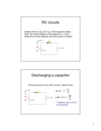
Switch Capacitor Filter Basic Theory • A simplified version on how a capacitor can work as a resistor by charting and recharges the capacitor by using a switch. • In practice the switch is replaced with two MOSFET, the gates of the MOSFET is controlled by two clock pulses which do not overlap each outer. • A switch capacitor resistor requires a very small silicon area to make a very large resistor value, if implement a resistant of 10M Ω , a good value of the capacitor will be in the range of 1pF to 10pF and a sample frequency around 100kHz. 1 1 = ⇒ = R 10M Ω • Capacitor of 1pF requires a silicon × × C f 1p 100k area around 0.01mm2 R S
Low-pass Switch Capacitor Filter V1 = 0 V2 V1 = 0 V3 V2 = 5 V2 = 5 TD = 0 TD = 500n R TR = 0 TR = 0 TF = 0 TF = 0 PW = 500n PW = 500n PER = 1u PER = 1u 1.592k 0 0 V1 VDB 1Vac C 0Vdc 10n VDB J1 J2 BC264A BC264A 0 0 V1 C2 1Vac C1 10n 0Vdc 628p 0 0 0
There are six ways to make a switch capacitor resistor Parallel. Bilinar. Q1 Q2 Q1 Q2 1 In Out = R × 1 Cs fs Q2 Q1 In Out = R Cs Cs × × 157p 628p 4 Cs fs 0 Series. Positive Transresistance Realization. Q1 Q1 Q1 Q2 C12 In Out 1 In Out 628p = R 1 × Q2 Q2 Cs fs = R Cs × Cs fs 628p 0 0 Series-Parallel. Negative Transresistance Realization. Q1 Q2 Q1 Q2 Cs In Out In Out 628p 1 1 Cs1 Q2 Q1 = = R R ( ) fs + × × Cs1 Cs2 Cs fs 528p Cs2 100p 0 0 0
State Variable Filter • One advantages of using SVF is that by changing the value of only a few components the parameters for the whole circuit is changed. • U1A and U1D performs as summing function, and U1B and U1C performs as integrators. dB Low-pass High-pass • R1 determine the gain for 0 Band-pass Band-reject -5 -3dB Series 1 the hole circuit. -10 -15 -20 • The ratio between R4 and -25 -30 R5 determined where the -35 -40 Centre frequency -45 -50 • The ratio between R6 -55 -60 and R7 specifics the -65 -70 value of Q. -75 -80 -85 frequenzy 1000 10000 100000
Switch Capacitor Filter Final Q1 Q2 +12Vcc V4 V5 V1 = 0 V1 = 0 V2 V2 = 5 V2 = 5 12Vdc TD = 0 TD = 500n TR = 0 TR = 0 TF = 0 TF = 0 PW = 500n PW = 500n Q1 Q2 PER = 1u PER = 1u 0 0 0 V3 12Vdc J1 J2 Q1 Q2 BC264A BC264A -12Vcc C3 J3 J4 100p BC264A BC264A C4 Q1 Q2 C1 -12Vcc Q1 Q2 C2 100p 10n 10n 11 J21 J22 TL084 -12Vcc VDB BC264A BC264A -12Vcc 2 C11 Q1 Q2 11 V- J5 J6 - TL084 VDB 62.5p BC264A BC264A 1 6 V1 11 OUT - V- TL084 1Vac C5 VDB 3 7 9 0Vdc 100p + V+ OUT - V- J23 J24 U1A 5 8 0 V+ 4 + OUT BC264A BC264A U1B C12 10 V+ 0 + 4 62.5p 0 U1C Q1 Q2 +12Vcc Q1 Q2 Q1 Q2 Q1 Q2 4 +12Vcc 0 +12Vcc J17 J18 J19 J20 J11 J12 J15 J16 BC264A BC264A BC264A BC264A BC264A BC264A BC264A BC264A C9 C10 C7 C8 100p 91p 100p 100p 0 0 0 0 -12Vcc Q1 Q2 11 TL084 VDB 13 - V- J7 J8 14 OUT BC264A BC264A C6 12 V+ + 100p U1D 4 0 0 +12Vcc
Switch Capacitor Filter output State Variable Filter with Switch Capacitor Final dB High-pass 5 Band-pass Low-pass 0 Band-reject -3 dB -40 dB -5 -10 -15 -20 -25 -30 -35 -40 -45 -50 -55 -60 -65 -70 -75 -80 -85 frequency 1000 10000 100000 1000000 10000000 1E8
Advantage & Disadvantage of Switch Capacitor Filter Advantage Disadvantage • Take up very little • Because the f S has to space of the chip area be 50 to 200 times bigger then the f C the • The accuracy of the SC filter technology capacitor it typically can’t be used at very within 0,1% high frequencies • Is very reliable for • Has to uses two clock temperature changes frequencies • Low supply use
Questions.
Recommend
More recommend
Explore More Topics
Stay informed with curated content and fresh updates.
