Session 6a: Bring us your coupons @Cornell ( Matthias Liepe , Yi Xie) - PowerPoint PPT Presentation
Session 6a: Bring us your coupons @Cornell ( Matthias Liepe , Yi Xie) TE host cavities with high surface fields ( 100 250 mT ) Q vs H Full T mapping of Bottom Plate 2 K Very good Hs/Hc ratios 1.4, 1.57 Pill box TE (Ready April)
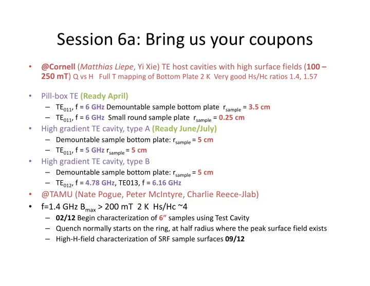
Session 6a: Bring us your coupons @Cornell ( Matthias Liepe , Yi Xie) TE host cavities with high surface fields ( 100 – • 250 mT ) Q vs H Full T mapping of Bottom Plate 2 K Very good Hs/Hc ratios 1.4, 1.57 Pill ‐ box TE (Ready April) • – TE 011 , f = 6 GHz Demountable sample bottom plate r sample = 3.5 cm – TE 011 , f = 6 GHz Small round sample plate r sample = 0.25 cm High gradient TE cavity, type A (Ready June/July) • – Demountable sample bottom plate: r sample = 5 cm – TE 011 , f = 5 GHz r sample = 5 cm High gradient TE cavity, type B High gradient TE cavity type B • • – Demountable sample bottom plate: r sample = 5 cm – TE 012 , f = 4.78 GHz , TE013, f = 6.16 GHz @TAMU (Nate Pogue, Peter McIntyre, Charlie Reece ‐ Jlab) @TAMU (Nate Pogue, Peter McIntyre, Charlie Reece Jlab) • f=1.4 GHz B max > 200 mT 2 K Hs/Hc ~4 • – 02/12 Begin characterization of 6” samples using Test Cavity – Quench normally starts on the ring, at half radius where the peak surface field exists – High ‐ H ‐ field characterization of SRF sample surfaces 09/12
Session 6b: Existing Facilities • @SLAC ( Tsyoshi Tajima ‐ LANL et al. ) 2” diam. Disk – 11.4 GHz 50 MW Klystron 11.4 GHz 50 MW Klystron – short pulses ( ≤ 2 μ s) – can separate thermal effect from critical field – TE 013 ‐ mode Cu hemispherical host cavity (cryocooled) – Q vs T already compared for ref Nb vs MgB 2 coating
Coupon Experiments Coupon Experiments • Relatively low cost y – Multiple variants – fast turnaround 2 or 3 per week? – Community needs to guide priorities – Q droop still possible with high Hs/Hc Q d till ibl ith hi h H /H • Re ‐ use instrumentation – tmapping etc. • Small samples = easier to control • Small samples = easier to control – Easier to characterize afterwards by microscopic techniques • Are they representative enough of “real” cavities? – Flat sheet vs cavity – Opportunity as well as hinderance Opportunity as well as hinderance
Session 6c: “Microscopic techniques” @Jlab (Larry Phillips, Daniel Bowring) Local Electronic Mean Free Path Niobium • : measurement of R s at various frequencies ω i Possible application to defect scanning in Nb sheet. pp g – Superconducting coaxial resonator in TEM modes. • Resonator and variable coupler are S.C. Nb with sapphire – dielectric and are conduction cooled in vacuum to 2K. – Measurements of R s at various frequencies allows a tomographic reconstruction of L e (x) Measurements of R s at various frequencies allows a tomographic reconstruction of L e (x). – (Preliminary) finite element simulation using CST, electric field at ~28 GHz. • Any sufficiently high ‐ Q resonator material can be used instead of 2 K Nb. • Not as good as magnetometer for ferromagnetic defects. • Simultaneous multiple frequencies provide better sensitivity. – @JLAB (Steven Anlage) Near ‐ field Microwave Microscopy Of Superconducting • Materials ‐ (Next Generation under development – utilize improvements in HD technology) ~1 µm ‐ stimulate Nb surface with large (B RF ~200 mT) RF field and induce nonlinear response. • Micro ‐ Loops (50 T pulses achieved!) • Laser Scanning Microscopy (Jlab collaboration (Karlsruhe) and FSU (Abraimov) have YBCO results) Laser Scannin Microscop (Jl b ll b ti (K l h ) d FSU (Ab i ) h YBCO lt ) • New Possibilities? Large surface coating MO? Large area PCT •
Recommend
More recommend
Explore More Topics
Stay informed with curated content and fresh updates.
