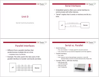
Serial QDR LVDS High-Speed ADCs on Xilinx Series 7 FPGAs Bruno - PowerPoint PPT Presentation
Serial QDR LVDS High-Speed ADCs on Xilinx Series 7 FPGAs Bruno Valinoti, Rodrigo Melo April 10th to April 12th, 2019, Buenos Aires Outline Introduction ADC board characteristics High Speed ADCs and the evolution next to FPGAs Proposal and
Serial QDR LVDS High-Speed ADCs on Xilinx Series 7 FPGAs Bruno Valinoti, Rodrigo Melo April 10th to April 12th, 2019, Buenos Aires
Outline Introduction ADC board characteristics High Speed ADCs and the evolution next to FPGAs Proposal and Implementation in the FMC16X IP Core Architecture for testing Validation and Results Conclusions X Southern Programmable Logic Conference
Proposed system ◮ Requirements, High speed, SNR and resolution. ◮ Abaco (4DSP) approach & problems ◮ Proposal ◮ Virtex 6 ◮ Zynq7000 series X Southern Programmable Logic Conference
Outline Introduction ADC board characteristics High Speed ADCs and the evolution next to FPGAs Proposal and Implementation in the FMC16X IP Core Architecture for testing Validation and Results Conclusions X Southern Programmable Logic Conference
Board specification FMC164 Analog Inputs Channels 4 Resolution 16 bits Input voltage range 1Vp-p (4dBm) to 2Vp-p (10 dBm) programmable Input gain Programmable from -2dB to 6dB in 0.5dB steps Input impedance 50 Ω Analog input bandwidth 500MHz (typical) ADC Output QDR LVDS mode; 4-pairs DDR per channel Output data width DDR LVDS mode; 8-pairs DDR per channel Data Format Offset binary or 2’s complement 250MHz internal clock Sampling Frequency Range Up to 250MHz external clock X Southern Programmable Logic Conference
ADC specifications ADS42LB69 Channels 2 Resolution 16 bits Input voltage range 2-V PP and 2.5-V PP Diff Full-Scale Input Maximum clock rate 250 MSPS SNR 72.3 dBFS @ 230MHz Output Interface DDR or QDR LVDS Input impedance 1.2k Ω (differential) X Southern Programmable Logic Conference
Framing features I DDR Clock D0 0 1 D2 2 3 D4 4 5 D6 6 7 D8 8 9 D10 10 11 D12 12 13 D14 14 15 N N+1 X Southern Programmable Logic Conference
Framing features II QDR Clock Frame D0 12 8 4 0 D1 13 9 5 1 D2 14 10 6 2 D3 15 11 7 3 N N+1 X Southern Programmable Logic Conference
Outline Introduction ADC board characteristics High Speed ADCs and the evolution next to FPGAs Proposal and Implementation in the FMC16X IP Core Architecture for testing Validation and Results Conclusions X Southern Programmable Logic Conference
Virtex II and Spartan 3 Scheme used in the application note XAPP774. D Q0 Q1 D Q Q Q Q Q Q Q2 Q3 ena E Q4 Mux & registers clk Q5 IOB D Q0 Q1 D Q Q Q Q Q Q Q2 Q3 ena_180 E Q4 clk_180 Q5 X Southern Programmable Logic Conference
Virtex 4 and Virtex 5 Scheme used in the application note XAPP866. X Southern Programmable Logic Conference
Virtex 6 The application note XAPP1071 shows a more sofisticated scheme: X Southern Programmable Logic Conference
Xilinx Series 7 The application note XAPP542 shows a very similar scheme like the XAPP1071. ISERDESE2 ISERDESE2 ISERDESE2 ISERDESE2 X Southern Programmable Logic Conference
Outline Introduction ADC board characteristics High Speed ADCs and the evolution next to FPGAs Proposal and Implementation in the FMC16X IP Core Architecture for testing Validation and Results Conclusions X Southern Programmable Logic Conference
Hardware connectios K J H G F E D C B A 1 ◮ FMC164 HA HA LA ◮ ZC706 LA ◮ FMC ◮ DDR vs QDR HB HB ◮ framing signals 40 LPC & HPC Only HPC To get 16-bit values with a sampling clock of 250 MHz, the clock provided by the ADC run at 500 MHz to read 4-bit as DDR two times, known as QDR mode. X Southern Programmable Logic Conference
IP Modules (I) ◮ adc_data.vhdl ◮ adc_frame.vhdl ◮ adc_cdc.vhdl ◮ adc_clock.vhdl X Southern Programmable Logic Conference
IP Modules (II) ◮ IBUFDS: differential input buffer. ◮ IDELAYE2: allows an input signal to be delayed. ◮ IDELAYCTRL: calibrates IDELAYE2, reducing effects of process, voltage, and temperature variations. ◮ ISERDESE2: a serial-to-parallel converter. ◮ IN_FIFO: very small FIFOs, designed for memory applications but available as general resource. ◮ ODDR: logic to implement an output DDR register. ◮ BUFG: global clock buffer. ◮ BUFIO: I/O clock buffer. ◮ BUFR: regional clock buffer. X Southern Programmable Logic Conference
Data deserializer IBUFDS x 4 Clock dat_p_i[3:0] ISERDESE2 x 4 Frame dat_n_i[3:0] D Q5...Q8 clk_i D0 12 8 4 0 CLK clk_div2_i CLKDIV bitslip_i D1 13 9 5 1 BITSLIP data_o[15:0] D2 14 10 6 2 Counter test_i D3 15 11 7 3 N N+1 X Southern Programmable Logic Conference
Syncronization and CDC (I) ◮ Forced bitslip input ◮ Signal shaping analysis, 1st order derivative ◮ Autoscale trigger ◮ Guard time ◮ Small FIFOs hardblocks near the IO X Southern Programmable Logic Conference
Syncronization and CDC (II) 30000 30000 15000 15000 0 0 15000 15000 30000 30000 36300 36550 36800 36300 36550 36800 14000 30000 15000 0 9500 15000 30000 5000 20000 22500 25000 20000 22500 25000 X Southern Programmable Logic Conference
Clocking IDELAYE2 clk_p_i IBUFGDS IDATAIN DATAOUT clk_n_i CE INC Control Different frequencies operating in FSM clk_o BUFIO the system, 500MHz in the IO, 250MHz in data deserialization and ISERDESE2 clk_div2_o BUFR 125MHz after the CDC. D Q1...Q8 %2 DDLY clk_div4 CLK O BUFR %4 CLKDIV X Southern Programmable Logic Conference
Outline Introduction ADC board characteristics High Speed ADCs and the evolution next to FPGAs Proposal and Implementation in the FMC16X IP Core Architecture for testing Validation and Results Conclusions X Southern Programmable Logic Conference
Design for testing the IP core REGS_to_AXIL GP AXIL AXI_DMA a F b AXIL HP M c M_AXI_S2MM d C S_AXIS_S2MM e 1 f 6 g X h AXIS AXIS axis_data_fifo test_fmc16x X Southern Programmable Logic Conference
Top level Ch A Ch A Core CLK A CLK A ADS42LB69 Ch B Ch B In order to be compatible with all Ch C Ch C the boards of the family, a set of Core ADS42LB69 Ch D Ch D generics are used enabling or Ch E Ch E disabling the resources by Core CLK E CLK E ADS42LB69 Ch F Ch F channels groups, depending on the Ch G Ch G board type. Core ADS42LB69 Ch H Ch H ANALOG DIGITAL FMC168/4/2 FMC168/4 FMC168 X Southern Programmable Logic Conference
Outline Introduction ADC board characteristics High Speed ADCs and the evolution next to FPGAs Proposal and Implementation in the FMC16X IP Core Architecture for testing Validation and Results Conclusions X Southern Programmable Logic Conference
Validation ◮ An internal fake data generator works muxed with SERDES to test the system, starting from the fifo’s inputs. ◮ Python scripts to analyze the fake data. ◮ Fast Fourier Transform of a well known signal being sampled. X Southern Programmable Logic Conference
Outline Introduction ADC board characteristics High Speed ADCs and the evolution next to FPGAs Proposal and Implementation in the FMC16X IP Core Architecture for testing Validation and Results Conclusions X Southern Programmable Logic Conference
Conclusions ◮ QuADC ◮ Base for the FMC10X IP Core ◮ Packet Standardization This work was co-funded by the European Union within the European Metrology Programme for Innovation and Research (EMPIR) joint research project 15SIB04 QuADC X Southern Programmable Logic Conference
Attribution-ShareAlike 4.0 International INTI-CMNB-FPGA http://creativecommons.org/licenses/ by-sa/4.0/ Bruno Valinoti valinoti@inti.gob.ar bruno-valinoti Rodrigo A. Melo Questions? rmelo@inti.gob.ar rodrigoalejandromelo @rodrigomelo9ok rodrigomelo9 Thanks! X Southern Programmable Logic Conference
Recommend
More recommend
Explore More Topics
Stay informed with curated content and fresh updates.
