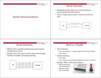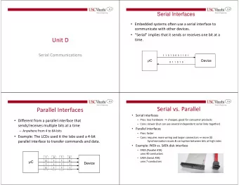
High-speed Serial Interface Lect. 1 Introduction 1 High-Speed - PowerPoint PPT Presentation
High-speed Serial Interface Lect. 1 Introduction 1 High-Speed Circuits and Systems Lab., Yonsei University 2013-1 What is interface? 2 High-Speed Circuits and Systems Lab., Yonsei University 2013-1 Interface application
High-speed Serial Interface Lect. 1 – Introduction 1 High-Speed Circuits and Systems Lab., Yonsei University 2013-1
What is “interface”? 2 High-Speed Circuits and Systems Lab., Yonsei University 2013-1
Interface application • Wireline/Wireless (Communication/Network ) PPPoE: Point-to-Point Protocol over Ethernet 3 High-Speed Circuits and Systems Lab., Yonsei University 2013-1
Interface application • Box to Box Laptop Audio Effector Audio Amp. Headphone 4 High-Speed Circuits and Systems Lab., Yonsei University 2013-1
Interface application • Rack to Rack (Inside data center) 5 High-Speed Circuits and Systems Lab., Yonsei University 2013-1
Interface application • Chip-to-chip – Inside your smartphone mipi: Mobile Industry Processor Interface LLI: Low Latency Interface SSIC: Super Speed InterChip UniPort: Unified Protocol UFS: Universal Flash Storage DigRF: Digital RF DSI: Display Serial Interface CSI: Camera Serial Interface D-PHY: 80Mbs to 1Gbps, no symbol coding, no CDR M-PHY: up to 5Gbps, 8B10B, CDR SLIMBus: Serial Low-Power Inter-Chip Media Bus SPMI: System Power Management Interface BIF: Battery Interface GBT: Giga Bit Trace RFFE: RF Front-End 6 High-Speed Circuits and Systems Lab., Yonsei University 2013-1
Why “high-speed”? VGA (1990’s) Resolution: 640 x 480 Color depth: 8bit Refresh rate: 60Hz 147Mb/s WQXGA (2010’s) Resolution: 2560 x 1600 Color depth: 24bit Refresh rate: 60Hz 5.9Gb/s 7 High-Speed Circuits and Systems Lab., Yonsei University 2013-1
Why “serial”? • Low-speed interface Tx Rx DATA Sampler Channel CLK Channel Ignorable skew 8 High-Speed Circuits and Systems Lab., Yonsei University 2013-1
Why “serial”? • How to increase data rate? – parallel interface – To parallelize / to increase clock speed – Increased skew / pin count Tx Rx DATA1 Sampler Channel DATA2 Sampler Channel DATAN Sampler Channel CLK Channel N+1 pins! Skew is not ignorable!! 9 High-Speed Circuits and Systems Lab., Yonsei University 2013-1
Why “serial”? • How to increase data rate? – serial interface – To send only high-speed data / to recover clock in Rx side – No skew problem / only 2 pin count Tx Rx DATA+ Channel Sampler Channel Skew is removed DATA- Only 2 pins Clock Recovery 10 High-Speed Circuits and Systems Lab., Yonsei University 2013-1
Why “serial”? • PCB traces: GMII (Gigabit Media Independent Interface) - Between Ethernet MAC to PHY Parallel interface Serial interface http://www.eetimes.com/design/communications-design/4142422/Going-Serial-in-Gigabit-Ethernet-Designs\ 11 High-Speed Circuits and Systems Lab., Yonsei University 2013-1
Block diagram • You will see this slide in (almost) every lecture! ☺ Tx Rx Serializer Channel Sampler Deserializer Driver Equalizer Clock PLL Recovery Tx Rx 12 High-Speed Circuits and Systems Lab., Yonsei University 2013-1
• Goals - Understand basics of high-speed serial interface - Learn how building blocks work - Design building blocks (In-Class Labs) - Learn advanced topics by surveying journal papers • Evaluation - Quiz: 3x10 = 30 - Lab Reports: 2x15 = 30 - Student Presentation: 2x15=30 - Class Participation: 10 • Class Hours - Mon 2:30-4 pm, Wed 1-2:30 pm • Lecturer Prof. Woo-Young Choi ( 최우영 ) - - Room: B625, Tel: 02-2123-2874 - wchoi@yonsei.ac.kr, tera.yonsei.ac.kr 13 High-Speed Circuits and Systems Lab., Yonsei University 2013-1
Syllabus (Tentative) Lect. 1: Introduction Lect. 2: Channel characteristics – 1 - ISI, Frequency dependent loss - Dielectric loss, skin effect, package parasitics, reflection Lect. 3: Channel characteristics - 2 - Time domain measurement 1- Oscilloscope / Eye-diagram - Time domain measurement 2 - TDR - Frequency domain measurement - S-parameter Lect. 4: Channel characteristics - 3 - Lumped element model - Transmission line model - S-parameter model Lect. 5: Equalizer - 1 - Continuous-time linear equalizer (CTLE) - Implementation Lect. 6. Equalizer - 2 - Discrete-time equalization - Decision-feedback equalizer (DFE) - Implementation Lect. 7.Channel Equalizer - 3 - Asynchronous equalizer adaptation - Synchronous equalizer adaptation - On-chip eye-diagram monitoring Lect. 8: Lab #1 - Behavioral-level design of CTLE and DFE Lect. 9-10: Student Presentation in English, Quiz 14 High-Speed Circuits and Systems Lab., Yonsei University 2013-1
Syllabus (Tentative) Lect. 11: Noises in high-speed serial link - Random noise, Power supply noise - Input offset, Crosstalk - BER, Bath-tub Lect. 12: Clocking structure - Clock distribution in system level - Source synchronous (Clock source in Tx side) - Plesiochronous(Clock source in both Tx and Rx side) - Embedded clocking (Clock recovery in Rx side) Lect. 13: Serializer/deserializer and low-power configuration - Binary-tree, FIFO, Mux - CMOS vs CML - Optimizing delay - Low-power configuration Lect. 14: Jitter - What is jitter? - Jitter characterization Lect. 15: Linear PLL dynamics - 1 - PLL block diagram - S-domain analysis - Jitter transfer function Lect. 16: Linear PLL dynamics - 2 - Stability analysis in s-domain - PLL bandwidth - Input and supply noise transfer Lect. 17: Charge-pump PLL - Block diagram - Effect of 3rd order loop filter - PFD, Charge pump, VCO, Divider Lect. 18: Phase noise analysis Lect. 19-20: Student Presentation in English, Quiz 15 High-Speed Circuits and Systems Lab., Yonsei University 2013-1
Syllabus (Tentative) Lect. 21: Clock and data recovery (CDR) - Why CDR? - Saw-filter - Over-sampling CDR - Gated-oscillator-based CDR - DLL-based CDR - PLL-based CDR Lect. 22: PLL/DLL-based CDR building blocks - Linear phase detector - Bang-bang phase detector - Dynamics analysis of CDR loop using bang-bang phase detector Lect. 23: Jitter in CDR - Category of jitter - RJ DJ DDJ BUJ - CDR Jitter characterization Lect. 24: Digital PLL - Digitally-controlled oscillator - Time-to-digital converter - Digital loop filter Lect. 25: Digital CDR - Difference from digital PLL - Digitalizing linear phase detector Lect. 26: LAB2 - Behavioral-level design of low SERDES, PLL, CDR Lect. 27-28: Student Presentation in English, Quiz 16 High-Speed Circuits and Systems Lab., Yonsei University 2013-1
Recommend
More recommend
Explore More Topics
Stay informed with curated content and fresh updates.
