PVMD Miro Zeman Delft University of Technology Crystalline silicon - PowerPoint PPT Presentation
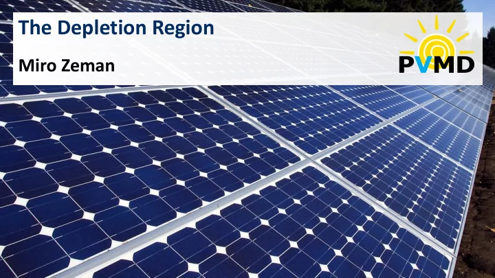
The Depletion Region PVMD Miro Zeman Delft University of Technology Crystalline silicon solar cell front contact n-type c-Si depletion region p-type c-Si absorber depletion region p ++ -type c-Si back contact Learning objectives
The Depletion Region PVMD Miro Zeman Delft University of Technology
Crystalline silicon solar cell front contact n-type c-Si depletion region p-type c-Si absorber depletion region p ++ -type c-Si back contact
Learning objectives ▪ Thermal equilibrium properties of P-N junction ▪ What is the depletion region ? ▪ How is the depletion region formed? ▪ Why is there an internal electric field in the depletion region?
Isolated doped silicon p -type Si n -type Si Charge neutral Charge neutral
P-N junction at thermal equilibrium p -type Si n -type Si metallurgical junction
P-N junction at thermal equilibrium p -type Si n -type Si N A = 10 16 cm -3 N D = 10 18 cm -3 > p = 10 16 cm -3 p ≈ 10 2 cm -3 Standard c-Si solar cells < n ≈ 10 4 cm -3 n = 10 18 cm -3
P-N junction at thermal equilibrium diffusion p -type Si n -type Si N A = 10 16 cm -3 N D = 10 18 cm -3 > p = 10 16 cm -3 p ≈ 10 2 cm -3 Standard c-Si solar cells < n ≈ 10 4 cm -3 n = 10 18 cm -3
P-N junction at thermal equilibrium diffusion p -type Si n -type Si Quasi-neutral region Depletion region Quasi-neutral region ρ qN D qN D qN A x
P-N junction at thermal equilibrium diffusion drift p -type Si n -type Si Quasi-neutral region Depletion region Quasi-neutral region ρ qN D qN D qN A x
P-N junction at thermal equilibrium diffusion drift p -type region n -type region Quasi-neutral region Depletion region Quasi-neutral region Electron Diffusion J e = qD e dn/dx J e = nq e E Electron Drift Hole Diffusion J h = qD h dp/dx J h = pq h E Hole Drift
Recommend
More recommend
Explore More Topics
Stay informed with curated content and fresh updates.

