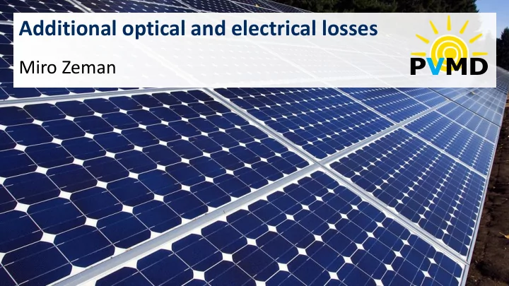
PVMD Miro Zeman Delft University of Technology Additional optical - PowerPoint PPT Presentation
Additional optical and electrical losses PVMD Miro Zeman Delft University of Technology Additional optical loss mechanisms 2 3 1 1. Shading Al Al n + 2. Reflection p-type 3. Parasitic absorption c-Si 3 4. Transmission p ++ p ++ Al
Additional optical and electrical losses PVMD Miro Zeman Delft University of Technology
Additional optical loss mechanisms 2 3 1 1. Shading Al Al n + 2. Reflection p-type 3. Parasitic absorption c-Si 3 4. Transmission p ++ p ++ Al 4
Shading losses The active area coverage factor, C f : Different patterns of front electrode Metal front electrode Semiconductor Metal back electrode
Shading losses and electrical losses Fingers Busbars R= Resistance ρ = resistivity L= length W= width H= height
Metal grid design
IBC Solar Cells sunpower
Reflection losses ~ ~ n Different refractive indices at interfaces n 1 2 Fresnel equation: 2 ~ ~ n n 1 2 R ~ ~ n n 1 2 Metal front electrode Exercise: λ =500nm Semiconductor ñ 1 =1+i0 (air) ñ 2 = 4.3+i0.045 (silicon) 2 3 . 3 i 0 . 045 R 0 . 31 Metal back electrode 5 . 3 i 004 . 5 7
Reducing Reflection n 0 ARC n 0 n 1 , d 1 ARC n 2 n 2 Semiconductor Semiconductor
Transmission losses Transmittance: exp T d c-Si (400 nm)=10 5 cm -1 (800 nm)= 10 3 cm -1 1 m of c-Si T(400 nm)=exp(-10 5 ×10 -4 )≈0 T(800 nm)=exp(-10 3 ×10 -4 )=0.90
Additional electrical losses: fill factor P max I P=I × V P V mp V oc V Peak Power P max [ W p ] FF = I mp I sc V I P V I FF mp mp Conversion efficiency max oc sc P P P I I I
Series Resistance (R S ) 200 Rs = 0 Ohm R S result of: Rs = 2.5 Ohm 100 Rs = 5 Ohm Rs = 7.5 Ohm Current Density [A/m 2 ] Rs = 10 Ohm ▪ 0 Bulk resistance of Rp = 1e4 Ohm semiconductor -100 ▪ Bulk resistance of metal electrodes -200 ▪ Contact resistance between -300 semiconductor and metal Voc Rs -400 0 0.1 0.2 0.3 0.4 0.5 0.6 0.7 0.8 Voltage [V]
Parallel Resistance (R p ) 200 Rp = 0.001 Ohm R P result of: Rp = 0.005 Ohm 100 Rp = 0.01 Ohm Rp = 0.03 Ohm Current Density [A/m 2 ] Rp = 1e4 Ohm 0 ▪ Leakage across P-N junction Rs = 0 Ohm around the edge Rp -100 ▪ Crystal defects, pinholes, -200 impurity precipitates -300 Voc -400 0 0.1 0.2 0.3 0.4 0.5 0.6 0.7 0.8 Voltage [V]
Collection loss Al Al n + p-type S = 10 4 cm/s c-Si S = 10 5 cm/s p ++ p ++ Al Bulk recombination Surface recombination S [cm/s] surface recombination velocity 1 1 1 U U [s -1 ]: recombination rate Effective minority carrier lifetime: n 13 bulk S
Recap Shading loss : ▪ metal electrode coverage R Reflection : ▪ different refractive indices Al Al Transmission and parasitic absorption: Transmission and parasitic absorption : FF ▪ finite thickness of a cell n + SiO 2 ▪ absorption coefficient ▪ supporting layers Fill factor, FF : IQE el ▪ Series and shunt resistances p-type c-Si p ++ p ++ Collection losses : ▪ bulk recombination Al ▪ surface recombination IQE op η g
Recommend
More recommend
Explore More Topics
Stay informed with curated content and fresh updates.

