PVMD Miro Zeman Delft University of Technology Reverse bias - + - PowerPoint PPT Presentation
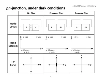
P-N Junction under Reverse Bias PVMD Miro Zeman Delft University of Technology Reverse bias - + V a I I C P N A I d Anode Cathode P-N junction at thermal equilibrium + - V a =0V E int - + p- type n- type diffusion drift P-N
P-N Junction under Reverse Bias PVMD Miro Zeman Delft University of Technology
Reverse bias - + V a I I C P N A I d Anode Cathode
P-N junction at thermal equilibrium + - V a =0V E int - + p- type n- type diffusion drift
P-N junction diode under reverse bias - + V a E int - + C A C p- type n- type diffusion drift
P-N junction diode under reverse bias - + V a E int - + C A C p- type n- type diffusion drift
Drift of minority carriers - + V a E int - + C A C p- type n- type diffusion drift 6
Current flow - + V a I I E int - + C A C Extremely small net dark current < diffusion drift injection Drift current is limited by minority carrier density
Thermal equilibrium Band diagram and voltage across the depletion region: V a = 0.0 V (Thermal equilibrium) p- type n- type p- type n- type 1.0 1.0 0.9 0.8 0.8 0.6 0.7 0.4 0.6 E F = E FN = E FP 0.2 Potential [V] Energy [eV] 0.5 0.0 0.4 -0.2 0.3 -0.4 0.2 -0.6 0.1 -0.8 0.0 -1.0 -1.2 -0.1 0.0 0.2 0.4 0.6 0.8 1.0 1.2 1.4 1.6 1.8 2.0 0.0 0.2 0.4 0.6 0.8 1.0 1.2 1.4 1.6 1.8 2.0 Position [µm] Position [µm]
Reverse bias = -0.1 V p- type n- type p- type n- type 1.0 1.0 0.9 0.8 0.8 0.6 0.7 0.4 0.6 E FP 0.2 Potential [V] Energy [eV] E C 0.5 0.0 0.4 -0.2 E FN 0.3 -0.4 0.2 -0.6 0.1 -0.8 E V 0.0 -1.0 -1.2 -0.1 0.0 0.2 0.4 0.6 0.8 1.0 1.2 1.4 1.6 1.8 2.0 0.0 0.2 0.4 0.6 0.8 1.0 1.2 1.4 1.6 1.8 2.0 Position [µm] Position [µm]
Recap Reverse Bias Thermal Equilibrium
Recommend
More recommend
Explore More Topics
Stay informed with curated content and fresh updates.







![The Schottky junction [Singh] Ideal case, no surface states Let consider n-silicon and a](https://c.sambuz.com/1031058/the-schottky-junction-singh-ideal-case-no-surface-states-s.webp)
