MTLE-6120: Advanced Electronic Properties of Materials Semiconductor - PowerPoint PPT Presentation
1 MTLE-6120: Advanced Electronic Properties of Materials Semiconductor p-n junction diodes Reading: Kasap 6.1 - 6.5, 6.9 - 6.12 2 Metal-semiconductor contact potential p -type n -type p -type n -type Same semiconductor on both sides,
1 MTLE-6120: Advanced Electronic Properties of Materials Semiconductor p-n junction diodes Reading: ◮ Kasap 6.1 - 6.5, 6.9 - 6.12
2 Metal-semiconductor contact potential p -type n -type p -type n -type ◮ Same semiconductor on both sides, different doping ◮ Bands line up perfectly, but Fermi level does not ◮ Bands bend to line up Fermi level ◮ Equal doping N a = N d ⇒ symmetric bending ◮ In general, contact potential shared between both sides ◮ Extreme limits: one side p + or n + , ∼ Schottky junction
3 Depletion region charge p -type n -type p -type n -type ◮ Far from junction, E F = E F 0 ⇒ ρ = 0 ◮ Approaching junction, E F first deviates ∼ k B T from E F 0 : Small deviation from neutral ⇒ Debye screening regime ◮ Once E F more than few k B T away from E F 0 (towards center of gap): n ≪ N d (or p ≪ N a ) ⇒ depletion; they were equal in neutral case ◮ Across junction, E F has to cross almost entire gap ≫ k B T ◮ Therefore, depleted width ≫ width where Debye screening applicable ◮ Assume ρ = + eN d for width w n on n -side, − eN a for width w p on p -side, and 0 elsewhere
4 Depletion region field and potential p -type n -type p -type n -type p -type n -type ◮ Neutrality of junction ⇒ N a w p = N d w n ◮ Solve for electric filed using ∇ · � E = E ′ ( x ) = ρ ( x ) /ǫ ◮ Solving from left, E ( x ) = − eN a ( w p + x ) /ǫ for x > − w p (0 otherwise) ◮ Solving from right, E ( x ) = − eN d ( w n − x ) /ǫ for x < w n (0 otherwise) ◮ Peak field E (0) = − eN a w p /ǫ = − eN d w n /ǫ ◮ Solve for potential using ∇ φ = φ ′ ( x )ˆ x = −E ( x )ˆ x to get: � eN a ( x + w p ) 2 , − w p ≤ x ≤ 0 2 ǫ φ ( x ) = eN a w 2 + eN a (2 xw n − x 2 ) p , 0 ≤ x ≤ w n 2 ǫ 2 ǫ
5 Depletion region width ◮ Total width w 0 ≡ w p + w n ; N a w p = N d w n ⇒ w p = w 0 N d w 0 N a N a + N d , w n = N a + N d ◮ Total potential across region: V 0 = eN a w 2 + eN a (2 w 2 eN a N d w 2 n ) p 0 = 2 ǫ 2 ǫ 2 ǫ ( N a + N d ) ◮ But total potential is the contact potential: � � � � E F 0 + k B T ln N d E F 0 − k B T ln N a = k B T ln N d N a eV 0 = − n 2 n i n i i � �� � � �� � E F n E F p ◮ Therefore depletion region width: � � 2 ǫ ( N a + N d ) V 0 2 ǫ ( N a + N d ) k B T ln N d N a w 0 = = n 2 eN a N d e 2 N a N d i ◮ When will depletion region width be set by λ D ?
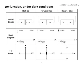
6 Applied bias p -type n -type ◮ Barriers for e − from n → p and holes from p → n : e ( V 0 − V ) ◮ Corresponding ‘diffusion’ current: j 2 exp − e ( V 0 − V ) k B T ◮ Junction field drives ‘drift current’: j 1 ◮ Must be balanced at V = 0 ⇒ j 1 = j 2 exp − eV 0 k B T ≡ j 0 � � ◮ Therefore j = j 0 eV exp k B T − 1
7 Magnitude of current ◮ So far IV -characteristics exactly like Schottky diode ◮ For Schottky diode, we found j 0 ∝ exp − Φ B k B T i.e. significant current when eV � Φ B ◮ For pn -junction diode at zero bias: equal drift and diffusion currents = j 0 ◮ Minority carrier diffusion current driven by concentration gradient ◮ In uniform n -semiconductor ˙ p = − ( p − p 0 ) /τ h (minority carrier lifetime τ h ) ◮ In non-uniform semiconductor: ˙ p = − D h ∇ 2 p (diffusion) ◮ Therefore in steady-state: D h ∇ 2 p = ( p − p 0 ) /τ ⇒ p decays exponentially towards p 0 with length scale L h = √ D h τ h = eD h n 2 ◮ Diffusion current j h = − eD h p ′ ( x ) ∼ eD h p 0 i L h L h N d ◮ Total minority diffusion current � D h � j 0 = eD h n 2 + eD e n 2 D e exp − E g i i = eN c N v + L h N d L e N a L h N d L e N a k B T ◮ Therefore current significant for V > E g /e
8 Minority carrier concentration in depletion region p -type n -type ◮ In n -depletion region, potential changes from neutral value by ( V 0 − V ) N a / ( N a + N d ) (maximum at junction) ◮ Assume symmetric doping, potential changes by ( V 0 − V ) / 2 ◮ Hole concentration at junction p M ∼ N a exp − e ( V 0 − V ) eV ∼ n i exp 2 k B T 2 k B T ◮ Hole recombination rate ∼ p M τ h · w n 2 (averaged over region)
9 Recombination current ◮ Current due to recombination of both e and h : � w n � + w p eV j r = en i exp τ h τ e 2 k B T ◮ Previous IV accounted for e and h transport separately, but not this recombination (except that it is needed for equilibrium) ◮ Net current density therefore: � eV � eV � � j ( V ) = j dd 0 k B T − 1 + j r 0 2 k B T − 1 ◮ Frequently approximated as � eV � j ( V ) = j 0 ηk B T − 1 with ideality factor η expected to be between 1 and 2 ◮ Ideal diode: no recombination ⇒ η = 1
10 Additional effects in reverse bias ◮ Space charge layer generation ◮ Reverse bias increases junction potential ◮ Higher field in space charge layer (depletion region) ◮ e and h in equilibrium: thermal generation vs recombination ◮ Field sweeps carriers away before they recombine ⇒ current ◮ Linearly increasing reverse current instead of saturated − j 0 ◮ Avalanche breakdown ◮ Depletion region: large field, few carriers ◮ If e E λ > E g , carriers can excite additional e-h pairs ◮ Cascade process leading to sudden increase in current ◮ Zener breakdown ◮ Highly doped junctions ⇒ narrow depletion regions ◮ Potential larger than E g : direct band-to-band tunneling ◮ Design sharp breakdown at specific potential (Zener diodes)
11 Depletion layer capacitance p -type n -type p -type n -type p -type n -type ◮ Charge stored = eN a w p = eN d w n = ew 0 N a N d / ( Na + N d ) (per unit area) ◮ Substituting for width of depletion region: � � q eN a N d 2 ǫ ( N a + N d )( V 0 − V ) 2 ǫeN a N d ( V 0 − V ) A = · = Na + N d eN a N d ( N a + N d ) ◮ Therefore differential capacitance: � C d ∂q ǫeN a N d A∂V = A ≡ 2( V 0 − V )( N a + N d ) ◮ Typical value for Si, N a = N d = 10 17 cm 3 , C ∼ 0 . 1 µ F/cm 2
12 Light-emitting diode ◮ Basic design: just a p - n junction, but in direct band-gap material ◮ Current density → recombination near junction ◮ Fraction of recombination is radiative ⇒ light ◮ Spontaneous emission: light is incoherent and in random direction ◮ Efficiency: η = P light / ( IV ) (can be > 10% for direct semiconductors) ◮ Typically use asymmetric junctions: pn + or np + : why?
13 LED: light spectrum ◮ Minimum photon energy: E g ◮ Peak photon energy ∼ E g + k B T ◮ Spectral width ∼ 3 k B T ◮ Due to distribution of both hole and electron energies ◮ For GaAs, E g = 1 . 42 eV, λ = 870 nm (IR) ◮ ∆( hc/λ ) ∼ 0 . 08 eV ⇒ ∆ λ ∼ 50 nm ◮ Light emitted by LED can be absorbed by semiconductor ◮ Circumvent in hetero-junction LEDs
14 Semiconductor laser ◮ Very similar to LED at the junction level ◮ Key difference: optical cavity using reflecting surfaces ◮ Start with spontaneous emission, sharpened by cavity resonance ◮ Stimulated emission builds up intensity in specific mode ◮ Require population inversion: e-h pairs waiting to recombine ◮ Population inversion achieved by bias: electrical pumping! ◮ Cavity resonance + laser amplification, ∆ λ ∼ 0 . 1 nm ≪ k B T
15 Photodiodes and solar cells ◮ LED in reverse? ◮ Not quite, can use indirect band gap materials ◮ Absorption still occurs right at band gap (how?) ◮ eh -pairs created in depletion region swept across by field ◮ Loss: recombination (radiative or non-radiative) ◮ Modified device characteristic � � eV j ( V ) = − j ph + j 0 exp ηk B T − 1 ◮ Why non-zero current at V = 0 if it is in equilibrium? ◮ Photodiode: operated in reverse bias: why?
16 Photovoltaic efficiencies Single junction efficiency limited by band-gap; circumvent using multi-junction devices S. Kurtz and D. Levi, NREL
Recommend
More recommend
Explore More Topics
Stay informed with curated content and fresh updates.




![The Schottky junction [Singh] Ideal case, no surface states Let consider n-silicon and a](https://c.sambuz.com/1031058/the-schottky-junction-singh-ideal-case-no-surface-states-s.webp)
