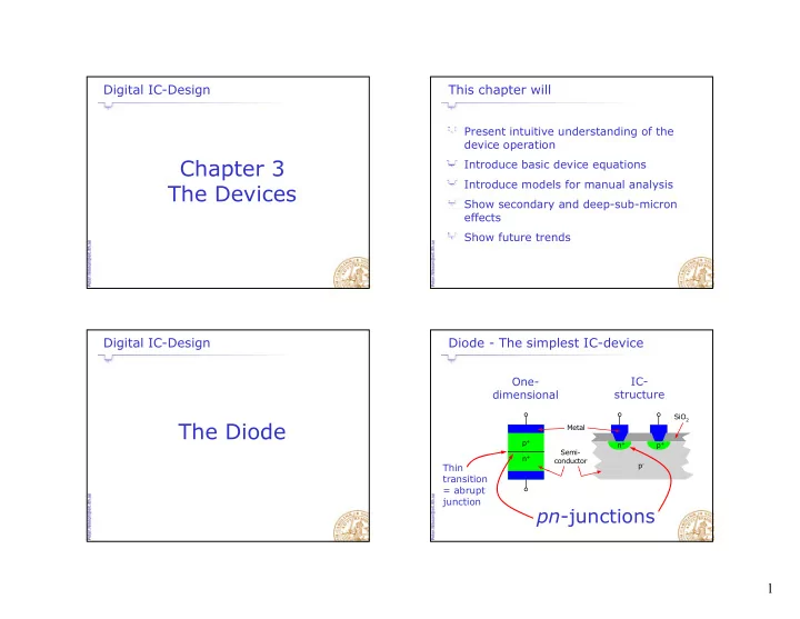

Digital IC-Design This chapter will Present intuitive understanding of the device operation device operation Chapter 3 Introduce basic device equations Introduce models for manual analysis The Devices Show secondary and deep-sub-micron effects effects Show future trends Digital IC-Design Diode - The simplest IC-device One- IC- dimensional structure SiO 2 The Diode Metal p + n + p + Semi- n + conductor Thin p - transition = abrupt junction pn -junctions 1
The Diode in an IC-device The Diode – Static Models Diodes appears reverse biased in all V D MOS-transistors e φ = × I I ( -1) T D S They have parasitics that affects the V D V D V Don performance (speed, power) Bonding Wire V DD Exponential First Order Protects input Protects input Model Model Pad To Core devices against Surface ”Protected” Fixed voltage static charges V Don “threshold” The Diode – a One Way Conductor The Diode – Dynamic Behavior The diode current I D has an exponential behavior Affects the maximum speed (how fast the regarding the voltage V D charges can be removed) V D e φ φ = × Aff Affects the dynamic power consumption t th d i ti I I ( -1) 2 5 2.5 T I D (mA) D S Diode Current 1.5 Forward biased p n + The diode can be seen as a capacitor Charge 0.5 density density Charges are built Charges are built Di t Distance Backward biased + 0 up around the pn - V D (V) junction - -0.5 -1 0 1 Forward “not allowed” 2
Junction Capacitance (abrupt junction) Junction capacitance – Example 3.3 Strongly non-linear capacitance Determine the junction capacitance for A = 0.5 μ m (junction area) μ 2 (j ) C j when V D C j when V D =0 0 C 0 C F F (derived at page 82) D D = j C F j V = × − 3 m 2 C 2 10 m − Φ (1 D ) 1/ 2 j 0 2 Φ = 0.64 V 0 C j when V D =-2.5 0 = − V 2.5 V D Small but billions of F = C = zero-bias capacitance in p (when ( V 0) ) them give a high g g C × × − 3 2 10 2 10 F F j j 0 0 2 2 D D m = j j 0 0 = = × − 3 3 C 0.9 10 total C − j V 2.5 m 2 − Φ 1/ 2 − 1/ 2 Φ (1 D ) (1 ) = built-in potential 0.64 0 0 = × = × − 12 × × − 3 = × − 15 = C A C 0.50 10 0.9 10 0.45 10 0.45 fF C j0 and Φ 0 are physical device parameters Diode D j Junction capacitance Example 3.3 - Continued Abrupt pn -junctions have a thin transition region Determine the junction capacitance for Integrated pn -junctions are often graded not abrupt b t C × − 2 10 3 F A linear transition region is often a better j 0 − = = = × 3 C 0.9 10 − − j abrupt V 2.5 2 m approximation − Φ − (1 ) 1/2 (1 ) 1/ 2 D 0.64 0 C F = j 0 C m j V 2 m − Φ 0 (1 ) D − C C × 3 3 Φ 2 10 2 10 F F = j 0 = = × − 3 C 1.2 10 − − j graded V 2.5 2 1 for abrupt m = − Φ 1/ 2 − 1/3 m p n -junctions (1 D ) (1 ) 2 0.64 0 1 for graded (linear) = m p n -junctions 3 3
Junction capacitance Junction capacitance Abrupt and graded junctions Strongly voltage dependent capacitance However, digital circuits tend to move fast b t between high and low voltages hi h d l lt = 2 4 A 0.5 μ m C (fF) D An equivalent (average) capacitance C eq can be F = × − C 2 10 m 3 used 3 j 0 2 Abrupt The same amount of charges is moved as by the Φ = 0.64 V 2 0 non-linear model Graded = − V 2.5 V D D Δ Q 1 = j = × C K C 0 (derived at page 83) eq Δ eq j V V D (V ) D 0 K eq is dependent on the grading coefficient m -5 -4 -3 -2 -1 0 0.6 Conclusion Diode Digital IC-Design Diodes appears in the drain and source areas (affects power and speed) Diodes should always be backward biased The MOS Transistor For digital design: the dynamic behavior is important A simple model for hand calculations can b be used in digital design: d i di it l d i = × C K C eq eq j 0 4
The MOS-transistor: An Old Invention What is a MOS-transistor? MOS = ”Metal Oxide Semiconductor” In 1925, Julius Edgar Lilienfeld described the first MOSFET structure Polysilicon Polysilicon - U.S. Patent in 1930 U S Patent in 1930 SiO 2 In early 30:es, a similar structure was shown by Oskar Heil Metal - British Patent in 1935 Silicon, doped Oxide None of them built a working component None of them built a working component Semiconductor The first working MOS-transistor was shown in early 60:es The MOS Transistor (or MOSFET) Simple Large Signal Model Most important device in digital design k = − 2 2 I I n n ( ( V V V V ) ) Very good as a switch V d i h D 2 GS T I D Relatively few parasitics = I Drain current Rather low power consumption D V DS = V Gate-Source voltage GS High integration density = = V V Drain Source voltage Drain-Source voltage DS V GS Simple manufacturing = V Threshold voltage T = k Gain factor (n-channel) Economical for large complex circuits n 5
How does it Work? What is a MOS Transistor? V GS must be A simple model: Opens a lager than a channel k A Switch Circuit Symbol threshold V T = = − 2 I I ( ( V V V V ) ) T D GS T 2 V GS V DS G V GS V GS G V DS drives a R eq I D S D S D current I D Gate Gate Source Drain Infinite resistance when V GS < V T R eq when V GS ≥ V T V T = Threshold voltage MOS – a Four Terminal Device Important Dimensions Technology Gate voltage determine the current from drain to source development: Gate Source connected to lower potential for n -channel devices ( (often to GND ) ) Drain Source Source 1993: 0.6 um Source connected to higher potential for p -channel devices W (often to V DD ) 2003: 65 nm t ox Bulk keeps the substrate at a stable potential. If not shown 2013: 18 nm? – it is assumed to be connected to the supply/ GND . Gate Gate L L Source Source Drain Drain Source Drain Bulk (Body) The technology is “Diode area” named after the Bulk (Body) gate length L 6
k MOS Circuit Symbols Simple Large Signal Model = − 2 I n ( V V ) D GS T 2 0.6 0.6 I D (mA) I D (mA) N-MOS P-MOS 0.4 0 4 0 4 0.4 Enhance- With Enhance- With ment Bulk ment Bulk 0.2 0.2 Enhance- Deple- Enhance- V GS (V) V GS (V) ment tion ment -1 0 1 2 3 -1 0 1 2 3 − − 6 6 × × 175 10 175 10 2 2 Drain Source = − = − − I ( V 0.5 ) I ( V ( 0.5 )) Gate Gate D GS D GS 2 2 Source Drain Enhancement Depletion Two Devices are Available - CMOS The Threshold Voltage V T The substrate is slightly doped (p - for NMOS) S V GS CMOS = Complementary MOS There are always free electrons in the substrate Static CMOS means complementary Static CMOS means complementary T f To form a channel, we need to attract these negative charges h l d t tt t th ti h G V DS NMOS/PMOS pairs The threshold is when the number of negative and positive Their gates are always connected charges are equal D pair wise The value of V T is thus set by the p -doping concentration Note that the corresponding V GS > V T D voltages ( V GS , V DS , V T …) for PMOS are voltages ( V ) for PMOS are V V negative G V DS That is, The PMOS transistor opens when the gate voltage is lower than n + n + V GS the source voltage S n -channel Depletion Region p - 7
The Bulk (Body) Potential The Threshold Voltage V T The bulk is most often connected to GND ( V DD for PMOS) = + γ − φ + − − φ V V ( 2 V 2 ) Negative V SB opens the diode; Not Allowed T T 0 F SB F Positi e V Positive V SB makes it harder to attract negative charges to makes it ha de to att act negati e cha ges to the channel φ F = Fermi potential That is, the threshold voltage will increase γ increases with the acceptor concentration V GS V SB Low threshold ⇒ Low voltage transistors but they are leaky y y Two threshold voltage technologies can be used p + n + n + for low power Strongly p-doped p - Threshold Voltage: Example 3.5 Threshold Voltage: Plot NMOS Determine the threshold voltage for a PMOS Twice the threshold for NMOS as well transistor with the following data: 0.9 = − V 0.4 V 0.85 0.85 T 0 Twice the γ = − 0.8 0.4 V threshold voltage! 0.75 = − V 2.5 V 0.7 SB V T (V) φ = 0.3 V 0.65 V T F 0.6 0.55 0.5 = + γ − φ + − − φ = V V ( 2 V 2 ) 0.45 T T 0 F SB F 0.45 0.4 = − − − − − − = V 0.4 0.4( 0.6 2.5 0.6 ) -2.5 -2 -1.5 -1 -0.5 0 T V BS (V) V SB = − V 0.79 V T 8
How does the MOS Work? (Cont.) How does it Work? When V GS is slightly increased When V GS is increased above V T Negative charges are attracted g g More negative than positive charges are attracted close to the gate (turns into n -type material) A Depletion region is formed A channel is formed (Strong inversion) V GS > 0 V GS > V T n + n + n + n + Depletion n -channel Depletion Region p - Region p - Linear Region (Resistive Operation) Linear Region (Resistive Operation) V DS is increased slightly I D ( V DS ) has a resistive behavior Horizontal E-field from drain to source I D has a linear relation to V GS D GS A current I D is established V GS > V T V DS <V GS -V T I D V GS > V T V DS <V GS -V T I D I D n + n + n n n -channel Depletion n + n + Region n -channel p - Depletion Region p - 9
Recommend
More recommend