Process Technology to Fabricate High Performance MEMS on Top of - PowerPoint PPT Presentation
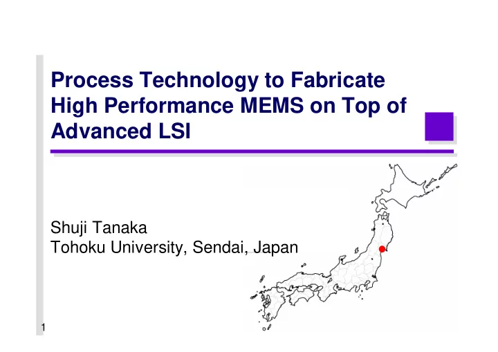
Process Technology to Fabricate High Performance MEMS on Top of Advanced LSI Shuji Tanaka Tohoku University, Sendai, Japan 1 JSAP Integrated MEMS Technology Roadmap More than Moore: Diversification Integrated 3 m inertia Integrated
Process Technology to Fabricate High Performance MEMS on Top of Advanced LSI Shuji Tanaka Tohoku University, Sendai, Japan 1
JSAP Integrated MEMS Technology Roadmap More than Moore: Diversification Integrated 3 µm inertia Integrated sensors Present health care High performance integrated devices More Moore: Miniaturization DMD sensors 0.8 µm Implantable devices Self-controlled ~2015 one-chip sensors One-chip multiband/ tunable ~2020 wireless chips Smaller More inteillent ~2025 More distributed Nanoelectronics 2
Multiband Wireless Communication W-LAN GSM/PDC W-LAN GSM/PDC 5.16 ~ 5.35 GHz 800 MHz 900 MHz 2.4 ~ 2.48 GHz 1.9 GHz W-CDMA Digital TV W-CDMA Digital TV 1.92 ~ 1.98 GHz UL 470 ~ 770 MHz 2.11 ~ 2.17 GHZ DL PHS WiMAX PHS WiMAX 1.88 ~ 1.92 GHz 2.5 ~ 2.7 GHz 4th Gen. 4th Gen. Tx Multi-band wireless Rx communication chip for W- CDMA + GSM/GPRS/EDGE (Qualcomm, QSC6240) 3
Integration of Wireless Communication System Unimplemented system Frequency tuning circuit Mixer Filter A/D Digital signal 0/90 º LNA processor A/D Rx Integrated devices based on RF CMOS technology Discrete devices Real one-chip solution enables not only advanced mobile communication systems but also ubiquitous network sensors, wireless healthcare chips etc. Integration of advanced LSI and “mechanical” devices (SAW/BAW filters, clock oscillators, RF MEMS switches, variable capacitors) is a key. 4
Inertia Sensors (Analog Devices) Safety steel ball sensor Detection circuit G sensor ADXRS150 2-axis gyro 1.3 μ m A tiny capacitance change (12 zF) corresponding to 125 μ m 1.6 × 10 -4 Å displacement is 2 μ m detectable by the embedded integrated circuit in the gyro. 5
Integrated Accelerometer (Analog Devices) Judy et al. , Hilton Head Island WS 2004, 27 On-CMOS structure Circuit Poly Si sensor structure (NPN, NMOS) Poly-Si sensor structure on 3 µm-ruled, W-metalized BiCMOS Poly-Si annealing at 1100 ° C for 30 min, Impossible to fabricate in LSI foundry SOI MEMS structure Trench isolation Sensor structure release Circuit from this trench Sensor structure SOI Single crystal Si sensor structure beside 0.6 μ m-ruled, Al-metalized CMOS Compatible with advanced LSI from LSI foundry, Low space efficiency 6
Digital Micromirror Device (TI) Hornbeck, IEDM 2007, 17-24 • 10~16 μ m square micromirrors • ~2 μ s response time • 8.5 V driving voltage • ± 12 ° tilt angle • 848 × 600 = 508800 pixels for SVGA ~ 1280 × 1024 = 1310720 pixels for SXGA 7
Applications of DMD Panasonic Rear-projection television Weight: 1 kg NEC NEC Projector for cinema Mobile projector complex 8
Metal Surface Micromachining for DMD (TI) Al Resist Resist 0.8 µm CMOS address 1. Sacrificial resist layer circuit Al SiO 2 (SRAM) 5. Sacrificial resist layer and Al mirror 2. Al and SiO 2 mask for hinges SiO 2 Al 6. Sacrificial resist etching 3. Al and SiO 2 mask for beams Kessel et al. , Proc. IEEE , 86 (1998) 4. Al etching for beams and hinges 9 1687 Hornbeck, IEDM 2007, 17-24
MEMS-LSI Integration using Ge Sacrificial Layer Collaboration with NDK • Multi-freq. AlN Lamb wave resonator monolithically integrated with LSI 1. Ge patterning and SiO 2 deposition Ge • Application to one-chip high-speed SiO 2 communication devices LSI 2. Metal patterning and AlN deposition Mo Al AlN LSI 3. AlN and Au/Cr patterning Au/Cr 310 MHz 4. Ge sacrificial etching 100 μ m 10
Electrostatic-Actuated Capacitive Shunt Switch On state Yuki et al. , Sensor Symposium 2007 Dielectric layer(SiO 2 ) Ni bridge 200 µm Ground Signal Off state Actuation pad Ground 20 0 Driving voltage: 38 V 15 -0.05 Insertion loss (dB) 10 -0.1 Notches for close contact Isolation (dB) 5 -0.15 Insert loss 0 -0.2 Sacrificial Sacrificial -5 -0.25 PR (3.5 µm) PR (1.5 µm) -10 -0.3 -15 -0.35 Isolation -20 -0.4 -25 -0.45 -30 -0.5 1 3 5 7 Freqency(GHz) Frequency (GHz) GND Signal GND 11
Wafer-Level Packaging of RF MEMS Switch Yuki et al. , Sensor Symposium 2007 Dry film Polyolefin mold resist 1. Molding dry film resist 4. Developing and over-coating Exposed part 2. Exposing dry film resist CPW Cavity CPW Dry film resist Exposed part DC in (Au/Cr) Device wafer 3. Laminating molded dry RF MEMS switch packaged by dry film resist and exposing film resist 12
Phase Shifter Using RF MEMS Switches Switching line type Reflection type Z 0 Z 0 Z 1 Capacitive Z shunt SW 2 Capacitive shunt SW 0 ° 22.5 ° SW down 45 ° 90 ° Reflect here 180 ° Reflection-type phase shifter SW up using RF MEMS switch Reflect here (Taiko Denki & Tohoku Univ.) 13
Memory Effect of Metal Hinges in DMD A. B. Southeimer, IEEE 40th Annual International Reliability Physics Symposium, Dallas, TX, 2002 Test duration Mirrors exhibiting hinge memory Shift (%) of bias voltage at which a half of mirrors land on the left side Duty cycle in accelerating test 50 % / 50% 5 % / 95% Simulating random image Simulating static image 14
Wafer Bonding-based MEMS-LSI Integration 1. Preparation of a device 4. Removal of the support Adhesion layer layer on a support wafer wafer/Thinning of the Device layer device wafer e.g.) Single Support wafer crystal Si, Interlayer LSI wafer Piezoelectric e.g.) SiO 2 , Polymer materials, 5. Fabrication of MEMS (e.g. Diamond, 2. Fabrication of a LSI wafer Compound RF MEMS switch, variable capacitor) or SAW/BAW semiconductors LSI wafer devices Electrical connection 3. Low temperature bonding of the device layer and the LSI wafer 6. Release of the device by Polymer sacrificial etching 15
Single Crystal RF MEMS Switch on Top of LSI Metal anchor Metal anchor Signal line Single crystal Si 200 μ m Actuation electrode cantilever Single crystal Si cantilever 25 Metal anchor OFF ON 20 Hight ( μ m) 15 10 OFF ( V drive = 0 V) 5 Single crystal Si 200 μ m ON ( V drive = 8 V) bridge 0 0 200 400 600 800 1000 RF MEMS switches on a dummy LSI wafer Lateral length ( μ m) 16
Single-Crystal-Si-on-LSI (SOL) Technology 1. Fabrication of metal pads 4. Patterning of metal 7. Removal of the on a (dummy) LSI wafer electrodes photoresist molds LSI wafer 2. Bonding a SOI wafer on 5. Shape formation of the the LSI wafer using 8. Sacrificial polymer etching device by reactive ion polymer interlayer by O 2 ashing to release etching the device SOI wafer Polymer 6. Cu electroplating using photoresist molds for 3. Etching of the handle and electrical connection Cu BOX layers 200 μ m Photoresist mold 17
AlN/Si Composite Resonators on Top of LSI 2. Mechanical-coupled AlN/Si 1. Electrically-coupled AlN/Si composite disk array filter composite thickness-mode filter In Out In Out SiO 2 Si Si GND GND λ 4 Coupling Beam AlN AlN Si Si Out-of-phase mode In-phase mode Collaboration with Mr. Matsumura (NiCT) 18
Single-Crystal-Si-on-LSI (SOL) Technology 5. Metal patterning 1. Wafer bonding using polymer SOI wafer Al Au/Cr Polymer LSI 2. Handle layer and BOX layer etching 6. Si etching Resist 3. Metal patterning Ru Au/Cr Au/T 7. Sacrificial polymer etching i 4. AlN deposition and patterning AlN SiO 2 19
AlN/Si Composite Resonators on Top of LSI Unpublished data 20
Share Wafer System in Tohoku University A Shuttle service A B C B Given process Registration from A Given process Registration from A D E F → Call for devices corp., B univ. … → Call for devices corp., B univ. … G H I Delivery Delivery Share wafer system after chip after chip separation separation Multiple devices Group A Group A in each shot Sensor circuit Sensor circuit A B D C Group B Group B Driver circuit Is there a Coordination Driver circuit A B Is there a Coordination common with LSI common with LSI A B D C process? foundry Group C process? foundry Group C Oscillator circuit Oscillator circuit D C Group D Group D Actuator circuit Actuator circuit MEMS fabrication Full wafers to MEMS fabrication Full wafers to each group by each group each group by each group 21 Project members (NDA is concluded.)
Summary • There is strong demands for monolithic integration of advanced LSI and “mechanical” devices such as clock oscillators, mechanical filters, switches and sensors. “More than Moore” with “Moore Moore” and “Biyond CMOS” • There are varieties of existing MEMS-LSI integration technology, but they are not suitable for the above applications. • We have developed new versatile microprocess technology for the monolithic integration of high-performance MEMS on top of advanced LSI. • Using the developed technology, we fabricated RF MEMS switches/variable capacitors, RF mechanical resonators and filters etc. Acknowledgement: This study was partly supported by Special Coordination Funds for Promoting Science and Technology. 22
Recommend
More recommend
Explore More Topics
Stay informed with curated content and fresh updates.
