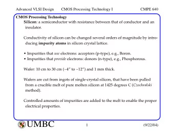
ME 645: MEMS: ME 645: MEMS: Design, Fabrication Design Fabrication - PDF document
Lecture 4: Lithography 1 ME 645: MEMS: ME 645: MEMS: Design, Fabrication Design Fabrication Design Fabrication Design, Fabrication and Characterization and Characterization P.S. Gandhi P.S. Gandhi Mechanical Engineering Mechanical
Lecture 4: Lithography 1 ME 645: MEMS: ME 645: MEMS: Design, Fabrication Design Fabrication Design Fabrication Design, Fabrication and Characterization and Characterization P.S. Gandhi P.S. Gandhi Mechanical Engineering Mechanical Engineering IIT Bombay IIT Bombay PRASANNA S GANDHI gandhi@me.iitb.ac.in PRASANNA S GANDHI gandhi@me.iitb.ac.in Recap: Last Class Recap: Last Class � Materials for MEMS Materials for MEMS � VLSI VLSI- -based fabrication processes: based fabrication processes: preliminary concepts preliminary concepts � Lithography Lithography � Material removal Material removal � Material addition Material addition � Combination of all these to make devices: Combination of all these to make devices: surface micromachining: Examples surface micromachining: Examples PRASANNA S GANDHI gandhi@me.iitb.ac.in PRASANNA S GANDHI gandhi@me.iitb.ac.in 1
Recap: Surface Recap: Surface Micromachining Micromachining U-V RAYS � Combination of Combination of lithography and etching lithography and etching � Defined with respect to Defined with respect to deposited films instead deposited films instead of Si substrate itself of Si substrate itself Wafer substrate PRASANNA S GANDHI gandhi@me.iitb.ac.in PRASANNA S GANDHI gandhi@me.iitb.ac.in Surface Micromachining Surface Micromachining Material Systems Material Systems Structural Sacrificial Release I solation Etch Polysilicon SiO 2 Buffered HF Si 3 N 4 + SiO 2 Polyimide Aluminum PAN etch SiO 2 LPCVD Si 3 N 4 Polysilicon XeF 2 SiO 2 + Al Aluminum Photoresist Oxygen SiO 2 plasma 2
Recap: HW Example Recap: HW Example � How will you make a � How will you make a How will you make a microchannels How will you make a microchannels microchannels on microchannels on on on � � surface of Si wafer using the processes surface of Si wafer using the processes learnt so far? What will be the masks? learnt so far? What will be the masks? � Can you control the shape of cross Can you control the shape of cross � section of section of microchannel microchannel? What way? ? What way? PRASANNA S GANDHI gandhi@me.iitb.ac.in PRASANNA S GANDHI gandhi@me.iitb.ac.in Microchannels Microchannels Mask geometry: PPR Mask geometry: PPR Exposure to U-V RAYS Developing Etching Removal of photoresist Substrate Wafer PRASANNA S GANDHI gandhi@me.iitb.ac.in PRASANNA S GANDHI gandhi@me.iitb.ac.in 3
Comments Comments � Exactly same process can be utilized to get more Exactly same process can be utilized to get more complex complex microchannel microchannel structures structures � We have assumed that etchant affects only the We have assumed that etchant affects only the top side however typically its on all sides and top side however typically its on all sides and hence protection of other sides necessary. Its hence protection of other sides necessary. Its usually done by oxidation process (oxide grows usually done by oxidation process (oxide grows everywhere) everywhere) � Q: How will you make fluid flow through these? Q: How will you make fluid flow through these? How to close the channels? Any ideas!! How to close the channels? Any ideas!! � How can we control the cross section? How can we control the cross section? We will now study these processes in depth We will now study these processes in depth PRASANNA S GANDHI gandhi@me.iitb.ac.in PRASANNA S GANDHI gandhi@me.iitb.ac.in Lithography: Types Lithography: Types � Optical lithography O ti O ti Optical lithography l lith l lith h h � Soft Lithography Soft Lithography � Electron beam lithography Electron beam lithography � X- -ray lithography ray lithography � Ion beam lithography Ion beam lithography � Dip Pen lithography � Dip Pen lithography Dip Pen lithography Dip Pen lithography 4
Lithography Lithography Positive Positive Photoresist Positive Positive Photoresist Photoresist (PPR) Photoresist (PPR) (PPR) (PPR) U-V RAYS MASK Wafer substrate Si, glass, etc. PRASANNA S GANDHI gandhi@me.iitb.ac.in PRASANNA S GANDHI gandhi@me.iitb.ac.in Some fundamental Some fundamental questions questions � Q: what affects the minimum feature that can Q: what affects the minimum feature that can Q: what affects the minimum feature that can Q: what affects the minimum feature that can be produced or transferred faithfully?? be produced or transferred faithfully?? � What is the chemistry of positive and negative What is the chemistry of positive and negative photoresists photoresists? Importance from resolution stand ? Importance from resolution stand point point � What are limits of this process? What are limits of this process? What are limits of this process? What are limits of this process? PRASANNA S GANDHI gandhi@me.iitb.ac.in PRASANNA S GANDHI gandhi@me.iitb.ac.in 5
Optical Lithography Optical Lithography I mportant parameters � Photoresist � Photoresist Photoresist Photoresist � Ways of exposure Ways of exposure � Contact printing Contact printing � Proximity printing Proximity printing � Projection printing Projection printing � Wavelength of light W Wavelength of light W l l th th f li ht f li ht � Intensity of light Intensity of light � Width w of the feature size: Diffraction effects Width w of the feature size: Diffraction effects Optical Lithography Optical Lithography Types � Contact printing � Contact printing Contact printing Contact printing � Proximity printing Proximity printing � Projection printing Projection printing What is the one we saw in animation? What is the one we saw in animation? 6
Contact Printing Contact Printing Process Adv/ Disadv � Mask pressed against resist (0 05 � Mask pressed against resist (0.05 Mask pressed against resist (0 05 Mask pressed against resist (0.05 – 0.3atm press) 0.3atm press) 0 3atm press) 0 3atm press) Very high resolution (< 1 μ m) possible � Very high resolution (< 1 m) possible � Flexible mask Flexible mask � Problems Problems � Nonuniform Nonuniform contact, resolution decreases contact, resolution decreases � Contact produces defects in mask and wafer (13 Contact produces defects in mask and wafer (13 def/cm2 after 5 exp � 37 def/cm2 after 15) : pinholes, def/cm2 after 5 exp 37 def/cm2 after 15) : pinholes, scratches, fractures etc. scratches, fractures etc. � Reduced mask life Reduced mask life Proximity Printing Proximity Printing � Need?? Motivation � Need?? Motivation Need?? Motivation Need?? Motivation � Contact printing problems Contact printing problems � Need to study some fundamentals of light to Need to study some fundamentals of light to understand understand � Limitations on feature size that can be produced Limitations on feature size that can be produced � Selection of process parameters to achieve min Selection of process parameters to achieve min feature size feature size 7
Fundamentals Fundamentals Proximity printing Animation: practical Animation: practical difficulties??? difficulties??? � Diffraction of light Diffraction of light Diffraction Limits Diffraction Limits � Assume Fresnel diffraction � Assume Fresnel diffraction Assume Fresnel diffraction Assume Fresnel diffraction Mask Wafer λ < < g < W < < g < W 2 / λ � Q factor Q factor 2 = Q W λ g w � Larger the Q more faithful x Larger the Q more faithful g g Q Q is the image is the image � Smaller the gaps g and Smaller the gaps g and g shorter the wavelength λ shorter the wavelength better the resolution better the resolution 8
Diffraction Limits Diffraction Limits � The effects of diffraction � The effects of diffraction The effects of diffraction The effects of diffraction are prominent at the are prominent at the corners corners � Solution: make Solution: make modifications in the mask modifications in the mask to get appropriate to get appropriate geometrical features geometrical features g � Another effect: standing Another effect: standing waves along thickness: waves along thickness: reflection from reflection from substrate � interference substrate interference Projection Printing Projection Printing � Projecting image of mask on the substrate � Projecting image of mask on the substrate Projecting image of mask on the substrate Projecting image of mask on the substrate � Expensive projection optics compatible to UV Expensive projection optics compatible to UV light necessary light necessary � Higher resolution than proximity printing Higher resolution than proximity printing � Larger separation between the mask and the Larger separation between the mask and the substrate substrate � Reduction while projecting so better for higher Reduction while projecting so better for higher resolution. Masks with lower resolution will do resolution. Masks with lower resolution will do for getting higher resolution. for getting higher resolution. 9
Masks for Masks for Lithography Lithography � Usually made up of glass substrate with Cr � Usually made up of glass substrate with Cr Usually made up of glass substrate with Cr Usually made up of glass substrate with Cr � For exposure at low frequencies quartz or Al For exposure at low frequencies quartz or Al 2 O 3 3 as as mask substrate have been used. mask substrate have been used. � Process of making masks??? Process of making masks??? � E- -Beam direct write lithography Beam direct write lithography Thank You Thank You PRASANNA S GANDHI gandhi@me.iitb.ac.in PRASANNA S GANDHI gandhi@me.iitb.ac.in 10
Recommend
More recommend
Explore More Topics
Stay informed with curated content and fresh updates.
