Microprocessors & Interfacing Computer buses I/O Addressing - PowerPoint PPT Presentation
Lecture Overview Buses Microprocessors & Interfacing Computer buses I/O Addressing Memory mapped I/O Buses and Parallel Separate I/O Input/Output Parallel Input/Output AVR examples Lecturer : Dr. Annie Guo
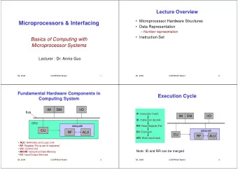
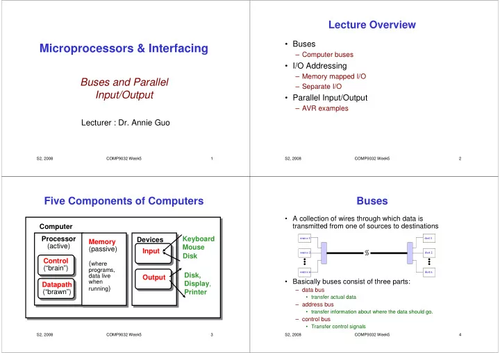
Lecture Overview • Buses Microprocessors & Interfacing – Computer buses • I/O Addressing – Memory mapped I/O Buses and Parallel – Separate I/O Input/Output • Parallel Input/Output – AVR examples Lecturer : Dr. Annie Guo S2, 2008 COMP9032 Week5 1 S2, 2008 COMP9032 Week5 2 Five Components of Computers Buses • A collection of wires through which data is transmitted from one of sources to destinations Computer Processor Keyboard Devices source 1 dest 1 Memory (active) Mouse (passive) Input source 2 dest 2 Disk Control ( where (“brain”) programs, source n dest n Disk, data live Output • Basically buses consist of three parts: when Display , Datapath running ) – data bus (“brawn”) Printer • transfer actual data – address bus • transfer information about where the data should go. – control bus • Transfer control signals S2, 2008 COMP9032 Week5 3 S2, 2008 COMP9032 Week5 4
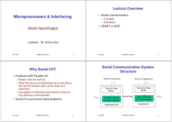
Typical Computer Bus Structure Computer Buses Parallel Serial • CPU is connected to memory and I/O devices I/O I/O via data, address and control buses. Device Device • Data bus is bi-directional and transfers information (memory data and instructions, I/O I/O data) to and from CPU. CPU Memory Interface • Address bus is most often unidirectional because CPU is the only source of the Data Bus addresses. Address Bus • Control bus carries all control signals required Control Bus to control the operation of the data transfer. S2, 2008 COMP9032 Week5 5 S2, 2008 COMP9032 Week5 6 Computer Buses (cont.) Input Interface • Connects multiple data sources • Each line of a bus has multiple sources and destinations. The bus transfers data from one – Only one source data is sent to the bus at a time • Often implemented with three-state buffers for source each time. data buses Multiple Destinations – For example, • a parallel, eight-bit input data is connected to eight three- • • • • • • • • • • • • state gates whose enable lines are tied together Data Bus • When the data is to sent to the bus the eight three-state CPU gates are enabled. • The open-collector gate is often used for control signals such as request for interrupts • • • • • • • • • • • • – Since one way switch is often required. Multiple Sources S2, 2008 COMP9032 Week5 7 S2, 2008 COMP9032 Week5 8
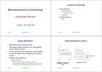
Typical Bus Interface Gates Output Interface Vcc • The output interface between the data bus Data source input Bus line and a destination or output device contains a A Y latch. External Pull-up G DBn Resistor Open G A Y D Q Collector Destination or 0 0 0 Output Device 74116 Dual 4-bit 0 1 1 Latch with Clear 1 0 X Clock 1 1 X C1 High Impedance C2 CLR (a) Three-state (b) Typical open-collector gate gate S2, 2008 COMP9032 Week5 9 S2, 2008 COMP9032 Week5 10 Address Decoding for Input Address Decoding Devices 74LS139 • The interface must provides the ability for 2-of-4 Decoder CPU to select one of many sources and A1 A1 From destinations. O0 CPU A0 A0 O1 – The address decoder is used. Read O2 E Control O3 Info Info Info Info Source Source Source Source To/From CPU Data Bus S2, 2008 COMP9032 Week5 11 S2, 2008 COMP9032 Week5 12
Address Decoding for Output CPU Timing Signals Devices 74LS139 • CPU must provide timing and synchronization 2-of-4 Decoder so that the transfer of information occurs at A1 A1 From the right time. O0 CPU A0 A0 O1 – CPU has its own clock. Write O2 E Control – I/O devices may have a separate I/O clock. O3 – Typical timing signals include READ and WRITE. 74116 74116 74116 74116 Dual 4-Bit Dual 4-Bit Dual 4-Bit Dual 4-Bit Latch Latch Latch Latch To/From CPU Data Bus S2, 2008 COMP9032 Week5 13 S2, 2008 COMP9032 Week5 14 Typical CPU Read Cycle Typical CPU Read Cycle • CPU places the address on the address bus CPU Clock at point A. • The control signal READ is asserted at point A Address B to signal the external device that CPU is address from CPU valid Bus ready to take the data from the data bus. C • CPU reads the data bus at point C whether Data Bus data from device valid or not the input device has put it ready – If NOT, some form of synchronization is required. READ Control Signal B S2, 2008 COMP9032 Week5 15 S2, 2008 COMP9032 Week5 16
Typical CPU Write Cycle Typical CPU Write Cycle • CPU places the address on the address bus at point CPU Clock A. • The data bits are supplied by CPU at point B. A • The control signal WRITE is asserted by CPU at Address address from CPU valid Bus point C to signal the external device that the data is ready to be taken from the data bus. B – This signal is used to create the clock to latch the data at the Data Bus data from CPU valid correct time. • Depending on the type of latch and when WRITE is WRITE asserted, the data may be captured on the falling Control Signal edge or rising edge. C D S2, 2008 COMP9032 Week5 17 S2, 2008 COMP9032 Week5 18 Complete I/O Interface Complete I/O Interface (cont.) Data Bus • READ and WRITE control the enable (E). 74LS139 • Three state enables and the latch clock 2-of-4 74LS244 Octal Decoder Buffer signals are not asserted until the correct A1 address is on the address bus AND the A1 SOURCE_ADR_OK O0 A0 correct time in the read or write cycle has A0 O1 Source READ O2 arrived. E O3 74116 Dual 4-Bit Latch Destination A1 DES_ADR_OK A1 O0 A0 A0 O1 WRITE O2 E O3 S2, 2008 COMP9032 Week5 19 S2, 2008 COMP9032 Week5 20
I/O Addressing Memory Mapped I/O • If the same address bus is used for both • The entire memory address space is divided memory and I/O, how does hardware into memory space and I/O space. distinguish between memory reads/writes and I/O reads/writes? – Two approaches: • Memory-mapped I/O. Memory • Separate I/O. – AVR supports both. I/O S2, 2008 COMP9032 Week5 21 S2, 2008 COMP9032 Week5 22 AVR Memory Mapped I/O Memory Mapped I/O (cont.) • In AVR, 64 I/O • Advantages: registers are mapped – Simple CPU design. into memory space – No special instructions for I/O accesses. $0020 ~ $005F • Disadvantages: – 2 bytes – I/O devices reduce the amount of memory space • With such memory available for application programs. addresses, the – The address decoder needs to decode the full address bus to avoid conflict with memory access to the I/Os addresses. uses memory access type of instructions. S2, 2008 COMP9032 Week5 23 S2, 2008 COMP9032 Week5 24
I/O Interface for Memory-Mapped Separate I/O I/O • Two separate spaces for memory and I/O. ADR_OK – Less expensive address decoders than those needed for memory-mapped I/O (Why?) Address to memory Bus Data Bus • Additional control signal, called IO/M, is required to prevent both memory and I/O ADR_OK Information trying to place data on the bus D Q Destination Decoder simultaneously. CL to input devices – IO/M is high for I/O use and low for memory use. Information ADR_OK Source • Special I/O instructions are required. READ to output devices WRITE S2, 2008 COMP9032 Week5 25 S2, 2008 COMP9032 Week5 26 I/O Interface for Separate I/O Separate I/O (cont.) Data Bus • In AVR, 64 I/O registers can also be addressed with separate addresses $00 ~ Reduced Address Bus $3F ADR_OK – 1 byte Decoder IO_READ • With such separate addresses, the access to the I/Os uses I/O specific instructions. Information Source - memory READ – E.g. IN and OUT IO/M Information Source – input device S2, 2008 COMP9032 Week5 27 S2, 2008 COMP9032 Week5 28
I/O Synchronization Software Synchronization • CPU is typically much faster than I/O devices. Two software synchronization approaches: • Real-time synchronization • Therefore, synchronization between CPU and – Uses a software delay to match CPU to the timing requirements of the I/O device. I/O devices is required. • The timing requirement must be known • Two synchronization approaches: • Sensitive to CPU clock frequency. • Waste CPU time. – Software synchronization. • Polling I/O – Hardware synchronization. – A status register, with a DATA_READY bit, is added to the device. The software keeps reading the status register until the DATA_READY bit is set. • Not sensitive to CPU clock frequency. • Still waste CPU time, but CPU can do other tasks. S2, 2008 COMP9032 Week5 29 S2, 2008 COMP9032 Week5 30 Handshaking I/O Input Handshaking Hardware • A hardware synchronization approach with control signal READY or WAIT. – For an input device, when CPU is asking for input data, the To CPU WAIT INPUT DEVICE input device will assert WAIT if the input data is NOT Wait State available. When the input data is available, it will deassert Logic WAIT. While WAIT is asserted, CPU must wait until this DATA_REQUEST control signal is deasserted. Data Register – For an output device, when CPU is sending output data via the data bus, the output device will assert WAIT if it is not INFO_ADD_OK Address Bus ready to take the data. When it is ready, it will deassert WAIT. While WAIT is asserted, CPU must wait until this READ control signal is deasserted. Data Bus S2, 2008 COMP9032 Week5 31 S2, 2008 COMP9032 Week5 32
Recommend
More recommend
Explore More Topics
Stay informed with curated content and fresh updates.
