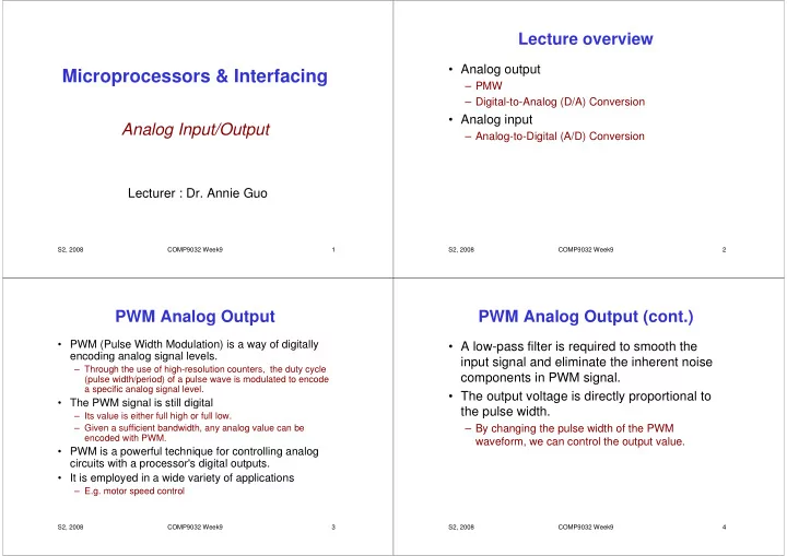
Microprocessors & Interfacing PMW Digital-to-Analog (D/A) - PowerPoint PPT Presentation
Lecture overview Analog output Microprocessors & Interfacing PMW Digital-to-Analog (D/A) Conversion Analog input Analog Input/Output Analog-to-Digital (A/D) Conversion Lecturer : Dr. Annie Guo S2, 2008 COMP9032
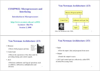
Lecture overview • Analog output Microprocessors & Interfacing – PMW – Digital-to-Analog (D/A) Conversion • Analog input Analog Input/Output – Analog-to-Digital (A/D) Conversion Lecturer : Dr. Annie Guo S2, 2008 COMP9032 Week9 1 S2, 2008 COMP9032 Week9 2 PWM Analog Output PWM Analog Output (cont.) • PWM (Pulse Width Modulation) is a way of digitally • A low-pass filter is required to smooth the encoding analog signal levels. input signal and eliminate the inherent noise – Through the use of high-resolution counters, the duty cycle components in PWM signal. (pulse width/period) of a pulse wave is modulated to encode a specific analog signal level. • The output voltage is directly proportional to • The PWM signal is still digital the pulse width. – Its value is either full high or full low. – By changing the pulse width of the PWM – Given a sufficient bandwidth, any analog value can be encoded with PWM. waveform, we can control the output value. • PWM is a powerful technique for controlling analog circuits with a processor's digital outputs. • It is employed in a wide variety of applications – E.g. motor speed control S2, 2008 COMP9032 Week9 3 S2, 2008 COMP9032 Week9 4
Examples of PWM Signals PWM Generation In AVR • PWM can be obtained through the provided Duty cycle=10% timers. Duty cycle=50% Duty cycle=90% S2, 2008 COMP9032 Week9 5 S2, 2008 COMP9032 Week9 6 Recall: Timer0 Configuration for PWM • TCCR0 S2, 2008 COMP9032 Week9 7 S2, 2008 COMP9032 Week9 8
CTC Fast PWM • Clear Timer on Compare Match S2, 2008 COMP9032 Week9 9 S2, 2008 COMP9032 Week9 10 Phase Correct PWM Example • Generate a PWM waveform. S2, 2008 COMP9032 Week9 11 S2, 2008 COMP9032 Week9 12
Example (solution) Example Code • Use Timer2 – Set OC2 as output .include "m64def.inc" – Set the Timer2 operation mode as Phase Correct .def temp=r16 PWM mode – Set the timer clock ldi temp, 0b10000000 out DDRB, temp ; Bit 7 will function as OC2. ldi temp, 0x4A ; the value controls the PWM duty cycle out OCR2, temp ; Set the Timer2 to Phase Correct PWM mode. ldi temp, (1<< WGM20)|(1<<COM21)|(1<<CS20) out TCCR2, temp S2, 2008 COMP9032 Week9 13 S2, 2008 COMP9032 Week9 14 Digital-to-Analog Conversion Digital-to-Analog Conversion (cont.) • A parallel output interface connects the D/A to the CPU. LATCH • The latches may be part of the D/A converter or the ENABLE output interface. Analog Output Digital-to- • Digital value is converted into continuous value. N N From CPU Signal Analog Latch Cond. Converter • A signal conditioning block may be used as a filter to Digital Data smooth the quantized nature of the output. – The signal conditioning block also provide isolation, buffering and voltage amplification if needed. S2, 2008 COMP9032 Week9 15 S2, 2008 COMP9032 Week9 16
Binary-weighted D/A Converter Quantized D/A Output – As the switches for the bits are closed, a weighted current is supplied to the summing junction of the 1.0 Desired amplifier. 0.8 sinusoid 0.6 – For high-resolution D/A converters, the binary- 0.4 weighted type must have a wide range of 0.2 resistors. This may lead to temperature stability 0 and switching problems. -0.2 -0.4 V D/A -0.6 B0 100K output -0.8 6.25K B1 50K -1.0 Analog - Output B2 25K + B3 12.5K S2, 2008 COMP9032 Week9 17 S2, 2008 COMP9032 Week9 18 R-2R Ladder D/A Converter D/A Converter Specifications – As a switch changes from the grounded position to • Resolution and linearity. the reference position, a binary-weighted current – The resolution is determined by the number of bits is supplied to the summing junction. and is given as the output voltage corresponding – For high-resolution D/A converters, a wide range to the smallest digital step, i.e. 1 LSB. of resistors are not required. – The linearity shows how closely the output voltage to the idea values (a straight line drawn through V REF zero and full-scale). • Settling Time. B0 B1 B2 B3 2R – The time taken for the output voltage to settle to 2R 2R 2R 2R within a specified error band, usually ± ½ LSB. Analog Output 2R R R R S2, 2008 COMP9032 Week9 19 S2, 2008 COMP9032 Week9 20
D/A Converter Specifications D/A Output Glitch (cont.) • Glitches. – A glitch is caused by asymmetrical switching in the D/A switches. If a switch changes from a one to a 10000000 zero faster than from a zero to a one, a glitch may Digital occur. Input • Consider changing the output code of a 8-bit D/A from Code 01111111 10000000 to 01111111 in the next slide. – D/A converter glitch can be eliminated by using a sample-and-hold. Glitch 00000000 t Output Voltage S2, 2008 COMP9032 Week9 21 S2, 2008 COMP9032 Week9 22 Deglitched D/A A/D Conversion physical electrical electronic electronic analog analog analog digital Trans- condi- Pro- ADC ducer tioner N Digital-to- Deglitched cessor Sample-and- Analog Analog Hold Converter Output Digital SAMPLE S2, 2008 COMP9032 Week9 23 S2, 2008 COMP9032 Week9 24
Data Acquisition and Conversion Data Acquisition and Conversion (Cont.) Procedure of data acquisition and conversion: • In applications where several analog inputs must be digitized, an analog multiplexer is followed the signal • A transducer converts physical values to electrical signals, either voltages or currents. conditioning. It allows multiple analog inputs, each • Signal conditioner performs the following tasks: with its own signal conditioning for different transducers. – Isolation and buffering: The input to the A/D may need to be protected from dangerous voltages such as static charges or • The sample-and-hold circuit samples the signal and reversed polarity voltages. holds it steady while the A/D converts it. – Amplification: Rarely does the transducer produce the voltage or current needed by the A/D. The amplifier is • The A/D converter converts the sampled signal to designed so that the full-scale signal from the analog results digital values. in a full-scale signal to the A/D. • The three state gates hold the digital values – Bandwidth limiting: The signal conditioning provides a low- pass filter to limit the range of frequencies that can be generated by the A/D converter. digitized. S2, 2008 COMP9032 Week9 25 S2, 2008 COMP9032 Week9 26 Data Acquisition System Shannon’s Sampling Theorem Claude Shannon’s Theorem: Signal Cond. Analog Input Transducer • When a signal, f(t) = X sin(2 π f sig t), is to be Analog Mux. sampled (digitized), the minimum sampling Other Analog Input frequency must be twice the signal frequency. Analog Multiplexer 2 THREE-STATE ENABLE N Analog-to-Digital N Sample- and- Converter Three State Gates Hold Data Digital TO CPU START_OF_CONVERT END_OF_CONVERT S2, 2008 COMP9032 Week9 27 S2, 2008 COMP9032 Week9 28
Sample Examples Sample Examples • Sampled at twice of the signal frequency. • Under-sampled, with sample frequency less than twice of the signal frequency 1.0 1.0 f(t)=Y sin(2 π g sig t) 0.8 0.8 f(t)=X sin(2 π f sig t) 0.6 A 0.6 0.4 A 0.4 0.2 0.2 0 0 -0.2 -0.2 -0.4 -0.4 B -0.6 B -0.6 -0.8 B -0.8 -1.0 -1.0 S2, 2008 COMP9032 Week9 29 S2, 2008 COMP9032 Week9 30 Shannon’s Sampling Theorem and Shannon’s Sampling Theorem and Aliasing Aliasing (Cont.) • To preserve the full information in the signal, • Undersampled signal, when converted back it is necessary to sample at twice the into a continuous time signal, will exhibit a maximum frequency of the signal. This is phenomenon called aliasing . known as the Nyquist rate . – Aliasing is the presence of unwanted components in the reconstructed signal. These components • A signal can be exactly reproduced if it is were not present when the original signal was sampled at a frequency F, where F is greater sampled. than or equal to the Nyquist rate. • If the sampling frequency is less than Nyquist rate, the waveform is said to be under- sampled. S2, 2008 COMP9032 Week9 31 S2, 2008 COMP9032 Week9 32
Successive Approximation Successive Approximation A/D Converter Converter • Each bit in the successive approximation register is tested, starting at the most significant bit and working toward the least Analog D/A Converter Ref significant bit. Input • As each bit is set, the output of the D/A Comparator Digital • converter is compared with the input. • MSB LSB • Outputs • If the D/A output is lower than the input signal, the bit remains set and the next bit is Successive Approximation tried. Clock Register • N times are required to set and test each bit in the successive approximation register. S2, 2008 COMP9032 Week9 33 S2, 2008 COMP9032 Week9 34 Parallel A/D Converter Parallel A/D Converter • An array of 2 N -1 comparators and produces Analog an output code in the propagation time of the Input Ref 2 N –1 comparators and the output decoder. Comparators R/2 5/6Ref • Fast but more costly in comparison to other + - designs. N outputs R • Also called flash A/D converter. 3/6Ref Digital + Decoder Outputs - R 1/6Ref + - R/2 S2, 2008 COMP9032 Week9 35 S2, 2008 COMP9032 Week9 36
Recommend
More recommend
Explore More Topics
Stay informed with curated content and fresh updates.

