Single-Cycle DataPath Lecture 15 CDA 3103 07-09-2014 Review of - PowerPoint PPT Presentation
Single-Cycle DataPath Lecture 15 CDA 3103 07-09-2014 Review of Virtual Memory Next level in the memory hierarchy Provides illusion of very large main memory Working set of pages residing in main memory (subset of all pages
Single-Cycle DataPath Lecture 15 CDA 3103 07-09-2014
Review of Virtual Memory • Next level in the memory hierarchy – Provides illusion of very large main memory – Working set of “ pages ” residing in main memory (subset of all pages residing on disk) • Main goal: Avoid reaching all the way back to disk as much as possible • Additional goals: – Let OS share memory among many programs and protect them from each other – Each process thinks it has all the memory to itself 2
Review: Paging Terminology • Programs use virtual addresses (VAs) – Space of all virtual addresses called virtual memory (VM) – Divided into pages indexed by virtual page number (VPN) • Main memory indexed by physical addresses (PAs) – Space of all physical addresses called physical memory (PM) – Divided into pages indexed by physical page number (PPN) 3
Review: Translation Look-Aside Buffers (TLBs) • TLBs usually small, typically 128 - 256 entries • Like any other cache, the TLB can be direct mapped, set associative, or fully associative hit VA PA TLB Main Processor miss Cache Lookup Memory miss hit data Trans- lation On TLB miss, get page table entry from main memory 7
Review: Memory Hierarchy Regs Upper Level Instr. Operands Faster Cache Blocks L2 Cache Blocks Last Week: Memory { Virtual Pages Memory Disk Files Larger Tape Lower Level 5
Review Example 1 A set-associative cache consists of 64 lines, or slots, divided into four-line sets. Main memory contains 4K blocks of 128 words each. Show the format of main memory addresses.
Solution The cache is divided into 16 sets of 4 lines each. Therefore, 4 bits are needed to identify the set number. Main memory consists of 4K = 2 12 blocks. Therefore, the set plus tag lengths must be 12 bits and therefore the tag length is 8 bits. Each block contains 128 words. Therefore, 7 bits are needed to specify the word.
Review Example 2 A two-way set-associative cache has lines of 16 bytes and a total size of 8 kbytes. The 64-Mbyte main memory is byte addressable. Show the format of main memory addresses.
Solution There are a total of 8 kbytes/16 bytes = 512 lines in the cache. Thus the cache consists of 256 sets of 2 lines each. Therefore 8 bits are needed to identify the set number. For the 64-Mbyte main memory, a 26-bit address is needed. Main memory consists of 64-Mbyte/16 bytes = 2 22 blocks. Therefore, the set plus tag lengths must be 22 bits, so the tag length is 14 bits and the word field length is 4 bits.
Agenda • Stages of the Datapath • Datapath Instruction Walkthroughs • Datapath Design Dr Dan Garcia
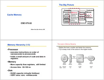
Five Components of a Computer Computer Keyboard, Mouse Devices Memory Processor Disk (passive) Input (where Control programs, (where data live programs, Output when not data live running) Datapath when running) Display , Printer Dr Dan Garcia
The CPU • Processor (CPU): the active part of the computer that does all the work (data manipulation and decision-making) • Datapath: portion of the processor that contains hardware necessary to perform operations required by the processor (the brawn) • Control: portion of the processor (also in hardware) that tells the datapath what needs to be done (the brain) Dr Dan Garcia
Stages of the Datapath : Overview • Problem: a single, atomic block that “executes an instruction” (performs all necessary operations beginning with fetching the instruction) would be too bulky and inefficient • Solution: break up the process of “executing an instruction” into stages, and then connect the stages to create the whole datapath – smaller stages are easier to design – easy to optimize (change) one stage without touching the others Dr Dan Garcia
Five Stages of the Datapath • Stage 1: Instruction Fetch • Stage 2: Instruction Decode • Stage 3: ALU (Arithmetic-Logic Unit) • Stage 4: Memory Access • Stage 5: Register Write Dr Dan Garcia
Stages of the Datapath (1/5) • There is a wide variety of MIPS instructions: so what general steps do they have in common? • Stage 1: Instruction Fetch – no matter what the instruction, the 32-bit instruction word must first be fetched from memory (the cache-memory hierarchy) – also, this is where we Increment PC (that is, PC = PC + 4, to point to the next instruction: byte addressing so + 4) Dr Dan Garcia
Stages of the Datapath (2/5) • Stage 2: Instruction Decode – upon fetching the instruction, we next gather data from the fields (decode all necessary instruction data) – first, read the opcode to determine instruction type and field lengths – second, read in data from all necessary registers • for add , read two registers • for addi , read one register • for jal , no reads necessary Dr Dan Garcia
Stages of the Datapath (3/5) • Stage 3: ALU (Arithmetic-Logic Unit) – the real work of most instructions is done here: arithmetic (+, -, *, /), shifting, logic (&, |), comparisons ( slt ) – what about loads and stores? • lw $t0, 40($t1) • the address we are accessing in memory = the value in $t1 PLUS the value 40 • so we do this addition in this stage Dr Dan Garcia
Stages of the Datapath (4/5) • Stage 4: Memory Access – actually only the load and store instructions do anything during this stage; the others remain idle during this stage or skip it all together – since these instructions have a unique step, we need this extra stage to account for them – as a result of the cache system, this stage is expected to be fast Dr Dan Garcia
Stages of the Datapath (5/5) • Stage 5: Register Write – most instructions write the result of some computation into a register – examples: arithmetic, logical, shifts, loads, slt – what about stores, branches, jumps? • don’t write anything into a register at the end • these remain idle during this fifth stage or skip it all together Dr Dan Garcia
§ 4.2 Logic Design Conventions Logic Design Basics Information encoded in binary Low voltage = 0, High voltage = 1 One wire per bit Multi-bit data encoded on multi-wire buses Combinational element Operate on data Output is a function of input State (sequential) elements Store information Chapter 4 — The Processor — 20
Combinational Elements AND-gate Adder A Y + Y = A & B Y = A + B B A Y B Arithmetic/Logic Unit Multiplexer Y = F(A, B) Y = S ? I1 : I0 A M I0 Y ALU Y u I1 x B F S Chapter 4 — The Processor — 21
§ 4.4 A Simple Implementation Scheme ALU Control ALU used for Load/Store: F = add Branch: F = subtract R-type: F depends on funct field ALU control Function 0000 AND 0001 OR 0010 add 0110 subtract 0111 set-on-less-than 1100 NOR Chapter 4 — The Processor — 22
Sequential Elements Register: stores data in a circuit Uses a clock signal to determine when to update the stored value Edge-triggered: update when Clk changes from 0 to 1 Clk D Q D Clk Q Chapter 4 — The Processor — 23
Sequential Elements Register with write control Only updates on clock edge when write control input is 1 Used when stored value is required later Clk Write D Q Write D Clk Q Chapter 4 — The Processor — 24
Clocking Methodology Combinational logic transforms data during clock cycles Between clock edges Input from state elements, output to state element Longest delay determines clock period Chapter 4 — The Processor — 25
§ 4.3 Building a Datapath Building a Datapath Datapath Elements that process data and addresses in the CPU Registers, ALUs, mux’s, memories, … We will build a MIPS datapath incrementally Refining the overview design Chapter 4 — The Processor — 26
Instruction Fetch Increment by 4 for next instruction 32-bit register Chapter 4 — The Processor — 27
R-Format Instructions Read two register operands Perform arithmetic/logical operation Write register result Chapter 4 — The Processor — 28
Load/Store Instructions Read register operands Calculate address using 16-bit offset Use ALU, but sign-extend offset Load: Read memory and update register Store: Write register value to memory Chapter 4 — The Processor — 29
Branch Instructions Read register operands Compare operands Use ALU, subtract and check Zero output Calculate target address Sign-extend displacement Shift left 2 places (word displacement) Add to PC + 4 Already calculated by instruction fetch Chapter 4 — The Processor — 30
Branch Instructions Just re-routes wires Sign-bit wire replicated Chapter 4 — The Processor — 31
Composing the Elements First-cut data path does an instruction in one clock cycle Each datapath element can only do one function at a time Hence, we need separate instruction and data memories Use multiplexers where alternate data sources are used for different instructions Chapter 4 — The Processor — 32
R-Type/Load/Store Datapath Chapter 4 — The Processor — 33
Full Datapath Chapter 4 — The Processor — 34
Generic Steps of Datapath registers rd instruction memory PC memory rs ALU Data rt imm +4 2. Decode/ 3. Execute 4. Memory 5. Register 1. Instruction Register Write Fetch Read Dr Dan Garcia
Recommend
More recommend
Explore More Topics
Stay informed with curated content and fresh updates.
