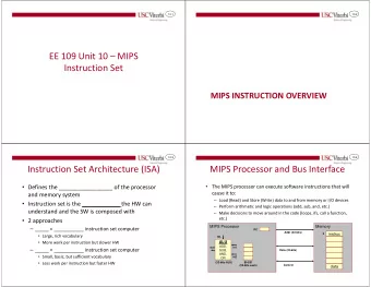
Lecture 6 Review Question #1 Calculate 999000999d * 3d 2997002997 - PowerPoint PPT Presentation
Lecture 6 Review Question #1 Calculate 999000999d * 3d 2997002997 Booth's Algorithm Use Booth's Algorithm to find 14d * -5d, in binary 01110 A = 01110 We need x 11011 B = 11011 5 + 5 = -B = 00101 10 bits A: 00000
Lecture 6 Review
Question #1 § Calculate 999000999d * 3d § à 2997002997
Booth's Algorithm § Use Booth's Algorithm to find 14d * -5d, in binary 01110 A = 01110 § We need x 11011 B = 11011 5 + 5 = -B = 00101 10 bits A: 00000 01110 (extend to 10 bits) ---------- 111011 0000 add +B (sign extend) + 0000 00101 0 add –B (sign extend) § à -70 ---------- 1110111010
Lecture 7 Review
Question #1 Address (PC) What is the Datapath of Instruction Instruction +4 Memory an r-type instruction Sign ext. Register File Mux Mux ALU Data Mux Memory Mux
Question #1 Address (PC) What is the Datapath of Instruction Instruction +4 Memory an r-type instruction Sign ext. Register File Mux Mux ALU ALU Data Mux Memory Mux
Question #2: Incrementing PC PCWriteCond Control PCSource PCWrite Unit ALUOp IorD ALUSrcB MemRead ALUSrcA MemWrite RegWrite MemtoReg RegDst IRWrite Opcode 0 1 2 Shift left 2 Instruction Registers [31-26] 0 Read Instruction PC 0 A reg 1 Address [25-21] Zero Read 1 A 1 Instruction data 1 Read Memory [20-16] reg 2 ALU data ALU Instruction result 0 Out Write Write Read [15-0] data reg B data 2 0 1 4 1 B ALU Write Instruction Memory 2 data Register 3 0 Memory 1 data Sign register Shift left 2 extend § Given the datapath above, what signals would the control unit turn on and off to increment the program counter by 4 ?
Controlling the signals § Need to understand the PCWriteCond PCSource PCWrite ALUOp role of each signal, and IorD ALUSrcB Control MemRead what value they need to ALUSrcA Unit MemWrite RegWrite have in order to perform MemtoReg RegDst IRWrite the given operation. § So, what’s the best approach Opcode to make this happen?
Basic approach to datapath 1. Figure out the data source(s) and destination. 2. Determine the path of the data. 3. Deduce the signal values that cause this path: Start with Read & Write signals (at most one a) can be high at a time). Then, mux signals along the data path. b) Non-essential signals get an X value. c)
Question #2: Incrementing PC PCWriteCond Control PCSource PCWrite Unit ALUOp IorD ALUSrcB MemRead ALUSrcA MemWrite RegWrite MemtoReg RegDst IRWrite Opcode 0 1 2 Shift left 2 Instruction Registers [31-26] 0 Read Instruction PC 0 A reg 1 Address [25-21] Zero Read 1 A 1 Instruction data 1 Read Memory [20-16] reg 2 ALU data ALU Instruction result 0 Out Write Write Read [15-0] data reg B data 2 0 1 4 1 B ALU Write Instruction Memory 2 data Register 3 0 Memory 1 data Sign register Shift left 2 extend § Step #1: Determine data source and destination. ú Program counter provides source, ú Program counter is also destination.
Question #2: Incrementing PC PCWriteCond Control PCSource PCWrite Unit ALUOp IorD ALUSrcB MemRead ALUSrcA MemWrite RegWrite MemtoReg RegDst IRWrite Opcode 0 1 2 Shift left 2 Instruction Registers [31-26] 0 Read Instruction PC 0 A reg 1 Address [25-21] Zero Read 1 A 1 Instruction data 1 Read Memory [20-16] reg 2 ALU data ALU Instruction result 0 Out Write Write Read [15-0] data reg B data 2 0 1 4 1 B ALU Write Instruction Memory 2 data Register 3 0 Memory 1 data Sign register Shift left 2 extend § Step #2: Determine path for data ú Operand A for ALU: Program counter ú Operand B for ALU: Literal value 4 ú Destination path: Through mux, back to PC
Question #3: Incrementing PC PCWriteCond Control PCSource PCWrite Unit ALUOp IorD ALUSrcB MemRead ALUSrcA MemWrite RegWrite MemtoReg RegDst IRWrite Opcode 0 1 2 Shift left 2 Instruction Registers [31-26] 0 Read Instruction PC 0 A reg 1 Address [25-21] Zero Read 1 A 1 Instruction data 1 Read Memory [20-16] reg 2 ALU data ALU Instruction result 0 Out Write Write Read [15-0] data reg B data 2 0 1 4 1 B ALU Write Instruction Memory 2 data Register 3 0 Memory 1 data Sign register Shift left 2 extend § Setting signals for this datapath: Read & Write signals: 1. PCWrite is high, all others are low.
Question #3: Incrementing PC PCWriteCond Control PCSource PCWrite Unit ALUOp IorD ALUSrcB MemRead ALUSrcA MemWrite RegWrite MemtoReg RegDst IRWrite Opcode 0 1 2 Shift left 2 Instruction Registers [31-26] 0 Read Instruction PC 0 A reg 1 Address [25-21] Zero Read 1 A 1 Instruction data 1 Read Memory [20-16] reg 2 ALU data ALU Instruction result 0 Out Write Write Read [15-0] data reg B data 2 0 1 4 1 B ALU Write Instruction Memory 2 data Register 3 0 Memory 1 data Sign register Shift left 2 extend § Setting signals for this datapath: Mux signals: 2. PCSource is 0 , AlUSrcA is 0 , ALUSrcB is 1 all others are “don’t cares”.
Question #2: Incrementing PC PCWriteCond Control PCSource PCWrite Unit ALUOp IorD ALUSrcB MemRead ALUSrcA MemWrite RegWrite MemtoReg RegDst IRWrite Opcode 0 1 2 Shift left 2 Instruction Registers [31-26] 0 Read Instruction PC 0 A reg 1 Address [25-21] Zero Read 1 A 1 Instruction data 1 Read Memory [20-16] reg 2 ALU data ALU Instruction result 0 Out Write Write Read [15-0] data reg B data 2 0 1 4 1 B ALU Write Instruction Memory 2 data Register 3 0 Memory 1 data Sign register Shift left 2 extend § Other signals for this datapath: ú ALUOp is 'ADD' (from chart on Slide 15 of Processor notes) ú PCWriteCond is X when PCWrite is 1 Otherwise it is 0 except when branching.
Question #2 (final signals) § PCWrite = 1 § PCSource = 0 § PCWriteCond = X § ALUOp = 'ADD' (001) § IorD = X § ALUSrcA = 0 § MemRead = 0 § ALUSrcB = 01 § MemWrite = 0 § RegWrite = 0 § MemToReg = X § RegDst = X § IRWrite = 0
Question #3 0000 0000 0110 0101 0100 0000 0010 0111 • What is the type of this instruction? • What does it do? • Which register stores the result?
MIPS instruction types § R-type: opcode rs rt rd shamt funct 6 5 5 5 5 6 § I-type: opcode rs rt immediate 6 5 5 16 § J-type: opcode address 6 26
0000 0000 0110 0101 Instruction Op/Func Instruction Op/Func add 100000 srav 000111 0100 0000 0010 0111 addu 100001 srl 000010 addi 001000 srlv 000110 addiu 001001 beq 000100 div 011010 bgtz 000111 divu 011011 blez 000110 mult 011000 bne 000101 multu 011001 j 000010 sub 100010 jal 000011 subu 100011 jalr 001001 and 100100 jr 001000 andi 001100 lb 100000 nor 100111 lbu 100100 or 100101 lh 100001 ori 001101 lhu 100101 xor 100110 lw 100011 xori 001110 sb 101000 sll 000000 sh 101001 sllv 000100 sw 101011 sra 000011 mflo 010010
Question #4 Give the binary representation of the op-code to add 0x4027 ( in decimal: 16423d ) to the value of r3, and put the result in r5
Instruction Op/Func Instruction Op/Func r5 ß r3 + 17 add 100000 srav 000111 addu 100001 srl 000010 addi 001000 srlv 000110 addiu 001001 beq 000100 div 011010 bgtz 000111 divu 011011 blez 000110 addi $5, $3, 16423 mult 011000 bne 000101 multu 011001 j 000010 sub 100010 jal 000011 subu 100011 jalr 001001 and 100100 jr 001000 00100000 01100101 andi 001100 lb 100000 nor 100111 lbu 100100 01000000 00100111 or 100101 lh 100001 ori 001101 lhu 100101 xor 100110 lw 100011 xori 001110 sb 101000 sll 000000 sh 101001 sllv 000100 sw 101011 sra 000011 mflo 010010
MIPS instruction types § R-type: opcode rs rt rd shamt funct 6 5 5 5 5 6 § I-type: opcode rs rt immediate 6 5 5 16 § J-type: opcode address 6 26
Pay Attention! § Very similar encodings produce difference results addi $5, $3, 16423 00 1 00000 01100101 01000000 00100111 00 0 00000 01100101 01000000 00100111 nor $8, $3, $5
Recommend
More recommend
Explore More Topics
Stay informed with curated content and fresh updates.


