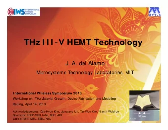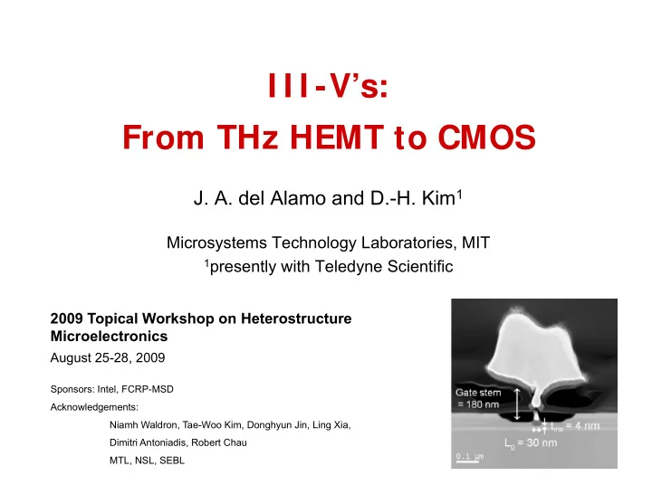
I I I -Vs: I I I V s: From THz HEMT to CMOS J. A. del Alamo and - PowerPoint PPT Presentation
I I I -Vs: I I I V s: From THz HEMT to CMOS J. A. del Alamo and D.-H. Kim 1 Microsystems Technology Laboratories, MIT 1 presently with Teledyne Scientific 2009 Topical Workshop on Heterostructure Microelectronics August 25-28, 2009
I I I -V’s: I I I V s: From THz HEMT to CMOS J. A. del Alamo and D.-H. Kim 1 Microsystems Technology Laboratories, MIT 1 presently with Teledyne Scientific 2009 Topical Workshop on Heterostructure Microelectronics August 25-28, 2009 Sponsors: Intel, FCRP-MSD Acknowledgements: Acknowledgements: Niamh Waldron, Tae-Woo Kim, Donghyun Jin, Ling Xia, Dimitri Antoniadis, Robert Chau MTL, NSL, SEBL 1
Outline • Introduction • Near-THz III-V HEMTs • Logic characteristics of III-V HEMTs • III-V CMOS • Conclusions 2
The High Electron Mobility Transistor Mimura, JJAPL 1980 3
Modulation doping • High electron mobility in modulation-doped AlGaAs/GaAs heterostructures • 2 DEG at AlGaAs/GaAs interface Dingle, APL 1978 Stormer, Solid St Comm 1979 4
HEMT circuits 27-stage ring oscillator E/D logic “The switching delay of 17 1 ps is the lowest of all 17.1 ps is the lowest of all the semiconductor logic technologies reported thus f far.” ” Mimura, JJAPL 1981 5
HEMTs in other material systems InAlAs/InGaAs on InP AlGaAs/InGaAs PHEMT K tt Ketterson, EDL 1985 EDL 1985 Kastalsky, APL 1982 1982 Also in AlGaN/GaN, Si/SiGe, AlSb/InAs, etc Also with holes in many heterojunction systems 6
HEMT Electronics: “You’ve come a long way baby!” ou e co e a o g ay baby 7
Near THz HEMTs • f T vs time: Kim EDL 2008 800 800 800 800 800 800 800 800 I I I -V HBTs I I I -V HBTs GHz] GHz] GHz] GHz] GHz] GHz] GHz] GHz] 600 600 600 600 600 600 600 600 I I I -V HEMTs I I I -V HEMTs equency [G equency [G equency [G equency [G equency [G equency [G equency [G equency [G 400 400 400 400 400 400 400 400 Cutoff Fre Cutoff Fre Cutoff Fre Cutoff Fre Cutoff Fre Cutoff Fre Cutoff Fre Cutoff Fre 200 200 200 200 200 200 200 200 SiGe HBTs SiGe HBTs SiGe HBTs SiGe HBTs Si CMOS Si CMOS 0 0 0 0 0 0 0 0 1985 1985 1985 1985 1985 1985 1985 1985 1990 1990 1990 1990 1990 1990 1990 1990 1995 1995 1995 1995 1995 1995 1995 1995 2000 2000 2000 2000 2000 2000 2000 2000 2005 2005 2005 2005 2005 2005 2005 2005 2010 2010 2010 2010 2010 2010 2010 2010 Year Year Year Year Year Year Year Year Year Year Year Year Year Year Year Year For over 20 years, f T (III-V’s) > f T (Si) 8
Near THz HEMTs • f T vs f max : 300 400 500 600 700 = f avg = f τ f 1000 1000 τ avg max max MIT HEMTs III-V HEMTs 800 III-V HBTs Kim IEDM 2008 ax [ GHz ] 600 400 400 f m 200 0 0 200 400 600 800 1000 f T [ GHz ] III-V HEMT: only device with f t , f max >600 GHz 9
I I I -Vs for CMOS? • Si scaling running into increasing difficulties: S D The scaled Si CMOS “performance gap” The scaled Si CMOS “performance gap” Courtesy of Dimitri Antoniadis (MIT) -15 G x 10 3 3 3 3 3 3 < Extrapolated > < Extrapolated > < Extrapolated > < Extrapolated > < Extrapolated > < Extrapolated > < Extrapolated > < Extrapolated > < Extrapolated > < Extrapolated > < Extrapolated > < Extrapolated > < < Historical > < < < Historical > < Historical > < < Historical > < Historical > < < Historical > < Historical Historical Historical Historical Historical Historical > > > > > > n) 2.5 2.5 2.5 2.5 2.5 2.5 2.5 2.5 2.5 2.5 rge (C/micro Delay (ps) Delay (ps) Delay (ps) Delay (ps) Delay (ps) Delay (ps) Delay (ps) Delay (ps) Delay (ps) Delay (ps) 1 2 2 2 2 2 2 2 2 2 2 “parasitic” charge 1 5 1.5 1.5 1.5 1.5 1 5 1.5 1.5 1.5 1 5 1.5 1 5 1 5 1 5 1 5 1 5 1.5 1 5 1 5 1.5 Intrinsic Intrinsic Intrinsic Intrinsic Intrinsic Intrinsic Intrinsic Intrinsic Intrinsic Intrinsic Gate Cha 0.5 1 1 1 1 1 1 1 1 1 1 channel charge 0.5 0.5 0.5 0.5 0.5 0.5 0.5 0.5 0.5 0.5 “15 nm” target “15 nm” target “15 nm” target “15 nm” target “15 nm” target “15 nm” target 15 nm target 15 nm target 15 nm target 15 nm target 15 nm target 15 nm target 0 0 0 0 0 0 0 0 0 0 0 0 20 40 60 80 100 120 0 0 0 0 0 0 0 0 0 0 20 20 20 20 20 20 20 20 20 20 40 40 40 40 40 40 40 40 40 40 60 60 60 60 60 60 60 60 60 60 80 80 80 80 80 80 80 80 80 80 100 100 100 100 100 100 100 100 100 100 120 120 120 120 120 120 120 120 120 120 CMOS Generation (nm) CMOS Generation (nm) CMOS Generation (nm) CMOS Generation (nm) CMOS Generation (nm) CMOS Generation (nm) CMOS Generation (nm) CMOS Generation (nm) CMOS Generation (nm) CMOS Generation (nm) CMOS Generation (nm) Parasitics becoming overwhelming � need higher current 10
Transistor as switch In logic applications transistor operates as switch Interested in : • ON current (I ON ) • OFF current (I OFF ) ( OFF ) • V T • V T dependence on L g • V T dependence on V DS (DIBL) • Subthreshold swing (S) • Device footprint • Gate capacitance • Operating voltage (V DD ) 11 11
How Do I I I -V FETs Look for Logic? Logic Characteristics of InGaAs High-Electron Mobility Transistor Kim, IEDM 2006 L g ~ 60 nm source gate drain Drain Source Source • Substrate is InP Substrate is InP InGaAs cap • Channel is In 0.7 Ga 0.3 As InAlAs insulator InP μ > 10 000 cm 2 /V s at 300K μ > 10,000 cm /V.s at 300K InGaAs channel • Barrier is In 0.52 Al 0.48 As InAlAs buffer 12 12
60 nm I nGaAs HEMT -3 0.5 10 I D V DS = 0.5 V I G V GS = 0.5 V -4 10 10 G GS 0.4 I d -5 V DS = 0.05 V 10 I D V GS = 0.4 V A/ μ m] 0.3 -6 10 mm] I D & I G [A I D [A/m -7 10 V GS = 0.3 V V DS = 0.5 V 0.2 I G I g -8 10 V GS = 0.2 V 0.1 -9 9 10 10 V GS = 0.1 V -10 0.0 10 0.0 0.2 0.4 0.6 0.8 -1.00 -0.75 -0.50 -0.25 0.00 0.25 0.50 V DS [V] V GS [V] Kim, IEDM 2006 At 0.5 V: V T = -0.02 V, S= 88 mV/dec, DIBL= 93 mV/V, I on /I off > 10 4 13 13
Benchmarking Against Si MOSFET: Gate Delay (CV/ I ) vs. L g Gate Delay (CV/ I ) vs L 10 For V at 1 μ A/ μ m For V T at 1 μ A/ μ m psec] E DELAY [p In 0.7 Ga 0.3 As HEMTs 1 (V DD = 0.5V) Kim, IEDM 2006 Kim IEDM 2006 GATE Si data from Chau, Si NMOSFETs T-Nano 2005 (V DD = 1.1~1.3V) 0.1 0 1 2 3 10 10 10 10 Gate Length, L g [nm] Gate delay comparable to Si, in spite of lower voltage 14 14
Benchmarking Against Si MOSFET: S & DI BL vs. L g S & DI BL vs L Kim, IEDM 2006 400 400 180 180 Si FETs (IEDM) InGaAs HEMTs InGaAs HEMTs Si FETs (IEDM) ope [mV/dec] ope [mV/dec] ] ] 160 160 300 300 140 140 mV/V] mV/V] 200 200 200 200 threshold Slo threshold Slo 120 120 120 120 DIBL [m DIBL [m 100 100 100 100 80 80 80 80 Sub Sub 0 0 60 60 10 10 100 100 10 10 100 100 Gate Length [nm] Gate Length [nm] Gate Length [nm] Gate Length [nm] At L g =60 nm, InGaAs HEMT as good as Si MOSFET � C � Can this device concept scale to the 15 nm node? thi d i t l t th 15 d ? � How will its performance compare with Si? 15 15
HEMT scaling • Key dimensions: L g , t ins , t ch , L side • Scaling trajectory: – L g ↓ � L g ↓ � • t ins ↓ • t ch ↓ • L side ? 16 16
I mpact of gate length 4 x 10 6 V DS = 0.5 V V DS =0.5 V 4 I OFF I ON / t ch = 13 nm 2 t ins = 10 nm L id = 150 nm L side 150 nm 0 0 100 200 300 400 500 L g [nm] • L g ↓ – I on /I off drops in the sub-200 nm regime p g on off – SCE worsen Kim, IEDM 2006 17 17
I mpact of barrier thickness 4 x 10 6 t ch = 13 nm V DS =0.5 V L side = 150 nm L 150 4 OFF I ON /I 2 t ins = 10 nm t ins = 6.5 nm t ins = 3 nm 0 0 100 200 300 400 500 L g [nm] • t ins ↓ – I on /I off worsens for long L g due to I G ↑ and R s ↑ g G ↑ s ↑ on off g – SCE and scalability improve Kim, IEDM 2006 18 18
I mpact of side recess length 5 200 10 V DS =0.5 V L side = 50 nm L side = 150 nm L side = 350 nm L = 350 nm 4 10 150 mV/dec] ON /I OFF t ch = 13 nm ch S [m I O 3 10 100 t ins = 10 nm L side = 50 nm L side = 150 nm L side = 350 nm side 2 10 50 0 100 200 300 400 0 100 200 300 400 L G [nm] L g [nm] • L side ↑ L Kim, ISDRS 2007 – I on /I off scalability improves – Better SCE B tt SCE – But… minimum L side shortens as t ins ↓ t ch ↓ 19 19
I mpact of channel thickness • t ch ↓ � performance degradation � increase InAs composition in channel 100 t ins = 3-4 nm InAs HEMTs dec] t ch = 10 nm L side = 150 nm 5 10 10 swing [mV/d 2 /V-s μ n = 13,000 cm 90 In 0.7 Ga 0.3 As HEMTs ON /I OFF 80 I O ubthreshold In 0.7 Ga 0.3 As HEMTs 70 InAs HEMTs t ch = 13 nm 2 /V-s V DS =0.5 V μ n = 10,000 cm V DS = 0.5 V DS S 4 10 60 100 10 100 L G [nm] L g [nm] • t ch ↓ + x(InAs) ↑ Kim, IEDM 2007 � I on /I off ↑ , better scalability, better SCE 20 20
Recommend
More recommend
Explore More Topics
Stay informed with curated content and fresh updates.
