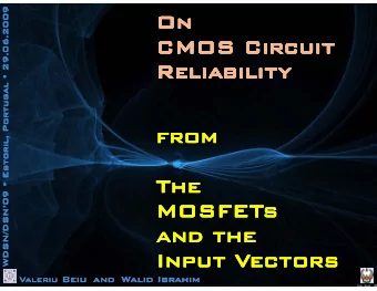
Highly Efficient GF (2 8 ) Inversion Circuit Based on Redundant GF - PowerPoint PPT Presentation
Saint-Malo, September 13th, 2015 Cryptographic Hardware and Embedded Systems Highly Efficient GF (2 8 ) Inversion Circuit Based on Redundant GF Arithmetic and Its Application to AES Design Rei Ueno 1 , Naofumi Homma 1 , Yukihiro Sugawara 1 ,
Saint-Malo, September 13th, 2015 Cryptographic Hardware and Embedded Systems Highly Efficient GF (2 8 ) Inversion Circuit Based on Redundant GF Arithmetic and Its Application to AES Design Rei Ueno 1 , Naofumi Homma 1 , Yukihiro Sugawara 1 , Yasuyuki Nogami 2 , and Takafumi Aoki 1 Joint work with 1 Tohoku University and 2 Okayama University
Outline Introduction Redundant GF arithmetic GF (2 8 ) inversion circuit AES encryption S-Box Concluding remarks 2
Background Demands for compact and efficient crypto. HW Applications to resource-limited devices in IoT Light-weight AES implementation www.hitachi.com Connectivity of existing systems and protocols Influence on other ciphers (e.g., Camellia, SNOW 3G) 3
AES processors GF (2 8 ) inversion is critical in AES processors Major part of SubBytes Round-based architecture Byte-serial architecture 38% delay of round datapath [Morioka+ 2004] 28% area of combinational block [Moradi+ 2011] Compact and efficient GF (2 8 ) inversion circuit is desirable 4
Design of GF (2 8 ) inversion circuit Arithmetic approach for AES S-box design Field towering and GF representation make a difference • Tower field: GF (((2 2 ) 2 ) 2 ) , GF ((2 4 ) 2 ) • GF representation: PB, NB, MB, RRB … Twisted-BDD, LUT, GF ((2 4 ) 2 ) SoP , PPRM, etc… Rudra+ Direct 2001 mapping PB GF (((2 2 ) 2 ) 2 ) Joen+ Area 2010 Satoh+ NB 2001 Nogami+ Nekado+ PB This 2010 2012 Tower field MB work Canright RRB 2005 NB Timing 5
Key trick Combination of three GF representations One non-redundant representation: Normal Basis (NB) Two redundant representations: • Polynomial Ring Representation (PRR) • Redundantly Represented Basis (RRB) RRB NB PRR Proposed circuit architecture 6
Results Highly efficient GF (2 8 ) inversion circuit Redundant GF arithmetic makes difference 38% faster than the conventional smallest one w/o area overhead Application to AES encryption S-box Isomorphic mappings optimized for efficiency 17% more efficient than state-of-the-art S-boxes Synthesis result of GF (2 8 ) inversion circuits with TSMC 65 nm Field Area [GE] Timing [ns] AT product GF (((2 2 ) 2 ) 2 ) [Canright 2005] 237.33 2.92 693.00 GF ((2 4 ) 2 ) [Nekado 2012] 272.67 1.89 515.35 This work GF ((2 4 ) 2 ) 229.67 1.81 415.70 7
Outline Introduction Redundant GF arithmetic GF (2 8 ) inversion circuit AES encryption S-box Concluding remarks 8
What’s redundant GF arithmetic? Represent GF (2 m ) element by n bits ( n > m ) Modular polynomial: n -th degree reducible polynomial Polynomial Ring Representation (PRR) Equal to Cyclic Redundancy Code (CRC) • D on’t -care inputs (explained by code theory) • Efficient for non-linear operations e.g., inversion Redundantly Represented Basis (RRB) Linear combination of linear dependent elements of GF (2 m ) • Each element is NOT represented uniquely • Efficient for multiplication 9
Why redundant GF arithmetic? Modular polynomial determines performance of GF arithmetic circuit Binomial x n + 1 is optimal but reducible Redundant GF can exploit binomial • x 5 + 1 is available for redundant GF (2 4 ) Critical factors of GF arithmetic algorithm Modular Rep. Squaring Multiplication Inversion polynomial PB Irreducible XOR-gate array Mastrovito ITA NB Irreducible Bit-wise permutation Massey-Omura ITA PRR Binomial Bit-wise permutation CVMA Mapping RRB Binomial Bit-wise permutation Reduced CVMA ITA 10
Why redundant GF arithmetic? Modular polynomial determines performance of GF arithmetic circuit Binomial x n + 1 is optimal but reducible Redundant GF can exploit binomial • x 5 + 1 is available for redundant GF (2 4 ) Critical factors of GF arithmetic algorithm Modular Rep. Squaring Multiplication Inversion polynomial PB Irreducible Bad OK OK NB Irreducible Good Bad OK PRR Binomial Good Good Good RRB Binomial Good Very good OK 11
Outline Introduction Redundant GF arithmetic GF (2 8 ) inversion circuit AES encryption S-Box Concluding remarks 12
Tower field inversion: Itoh-Tsujii Algorithm (ITA) GF ( q m ) inversion based on ITA is given by q -th power over GF ( q m ) is Frobenius mapping • Performed by cyclic shift in NB Usage of norm of input a • Considered as subfield ( GF ( q ) ) element • Inversion in rhs is GF ( q ) inversion ITA for GF ((2 4 ) 2 ) and GF (((2 2 ) 2 ) 2 ), i.e., q = 16, m = 2 a 16 calculated by only twisting wires a × a 16 is GF (2 4 ) element 13
ITA-based tower field inversion circuit Consists of 3 stages: Stage 1: 16th and 17th power Stage 2: GF (2 4 ) inversion Stage 3: final multiplication a 16 h l ( a 17 ) -1 a 17 Divided into GF (2 4 ) datapath 14
Area-Time efficiency evaluation NB -based GF (((2 2 ) 2 ) 2 ) inversion [Canright, 2005] NB NB NB 15
Area-Time efficiency evaluation RRB -based GF ((2 4 ) 2 ) inversion [Nekado, 2012] RRB RRB RRB 16
Proposed concept Use the best representation for each stage NB PRR RRB Input: PRR Input: NB Output: RRB Output: PRR, RRB 17
To avoid additional gates for conversion Mapping from NB to PRR is isomorphism Performed by applying linear mapping F to a 17 Merging F and constant multiplications in a 17 Stage 1 output d ( a 17 in PRR) given by • F ’ , F ’’ : merged linear mapping Symmetric property of GF (2 4 ) NB for h and l can further reduce Stage 1 delay Straight-forward mapping Asymmetric NB Symmetric NB T A + 5 T X T A + 4 T X T A + 3 T X T A , T X : delay of AND and XOR gate 18
Effect of PRR in Stage 2 Don’t -care condition of PRR is useful for GF (2 4 ) inversion function Field Representation Critical delay GF ((2 2 ) 2 ) PB 2 T A + 7 T X GF ((2 2 ) 2 ) NB 2 T A + 5 T X GF (2 4 ) PB 2 T A + 2 T X GF (2 4 ) NB 2 T A + 2 T X GF (2 4 ) RRB 2 T A + 2 T X GF (2 4 ) PRR T A + T O + T X T A , T O , T X : delay of AND, OR, and XOR gate Conversion from PRR to RRB can also be performed without logic gates 19
Proposed circuit RRB NB PRR Inputs to stage 1 and 3 should be shared H , L , and F are shared XOR-gate array To save 22 XOR gates NBtoRRB converts element from NB to RRB Performed by only wiring 20
Performance evaluation Gate count Tower Represen Critical (AND, OR, XOR, XNOR, Field -tation delay path NOT, NAND,NOR) GF (((2 2 ) 2 ) 2 ) Satoh et al. PB (30, 0, 96, 0, 0, 6, 0) 4 T A + 17 T X GF (((2 2 ) 2 ) 2 ) Canright NB (0, 0, 56, 0, 0, 34, 6) 4 T A + 15 T X Nogami et al. GF (((2 2 ) 2 ) 2 ) PB, NB (36, 0, 95, 0, 0, 0, 0) 4 T A + 14 T X Rudra et al. GF ((2 4 ) 2 ) PB (60, 0, 72, 0, 0, 0, 0) 4 T A + 10 T X Jeon et al. GF ((2 4 ) 2 ) PB (58, 2, 67, 0, 0, 0, 0) 4 T A + 10 T X GF ((2 4 ) 2 ) Nekado et al. RRB (42, 0, 68, 2, 0, 0, 0) 4 T A + 7 T X NB, PRR, GF ((2 4 ) 2 ) This work (38, 16, 51, 0, 4, 0, 0) 3 T A + T O + 6 T X RRB T A , T O , T X : D elay of AND, OR, and XOR gate Shortest critical delay path Gate count comparable with the conventional smallest 21
Synthesis result Synthesis with area optimization Logic synthesis: Design Compiler, Synopsys Cell Library: Standard 65 nm, TSMC Represent Area Timing AT Tower Field ation [GE] [ns] product GF (((2 2 ) 2 ) 2 ) Canright* NB 237.33 2.92 693.00 Nekado et al.** GF ((2 4 ) 2 ) RRB 272.67 1.89 515.35 NB, PRR, GF ((2 4 ) 2 ) This work 229.67 1.81 415.70 RRB *HDL code was obtained from Canright’s website **HDL code was described by ourselves according to the paper Our inversion circuit achieved the best efficiency (i.e. AT product) and area 22
Outline Introduction Redundant GF arithmetic GF (2 8 ) inversion circuit AES encryption S-Box Concluding remarks 23
AES encryption S-box Require isomorphic mappings and affine trans Later matrix operations should be merged Tower field AES field AES field Conversion matrices optimization for efficiency Hamming weight of each row should be less than 4 Hamming weight = 4 Hamming weight = 5 24
Synthesis result Critical delay path Area Timing AT [GE] [ns] product Iso. -1 +Affine Iso. Inversion Canright 315.67 4.30 1,357.38 3 T X 4 T A + 15 T X 3 T X Nekado et al. 386.00 3.29 1,269.94 2 T X 4 T A + 7 T X 3 T X This work 332.00 3.17 1,052.44 2 T X 3 T A + T O + 6 T X 3 T X Our S-Box achieved the highest efficiency Synthesis with area-optimization option Optimization of conversion matrix operations Canrights ’ are optimized for low -area Nekados ’ and ours are optimized for efficiency • Low-area optimization of our S-box is a future work 25
Concluding remarks Highly efficient GF (2 8 ) inversion circuit 38% faster than the conventional one w/o area overhead AES encryption S-Box with isomorphism optimization for efficiency Achieved the lowest Area-Time product Future work Further optimization of conversion matrices • Lower-area or/and higher efficiency • Both encryption and decryption S-box Design of AES datapath with the proposed S-box 26
Recommend
More recommend
Explore More Topics
Stay informed with curated content and fresh updates.









![Sorting is removing inversions. In an array sorted by ( ! ) we have [ ] ! [ ] ( ) i j ,](https://c.sambuz.com/828639/sorting-is-removing-inversions-s.webp)
