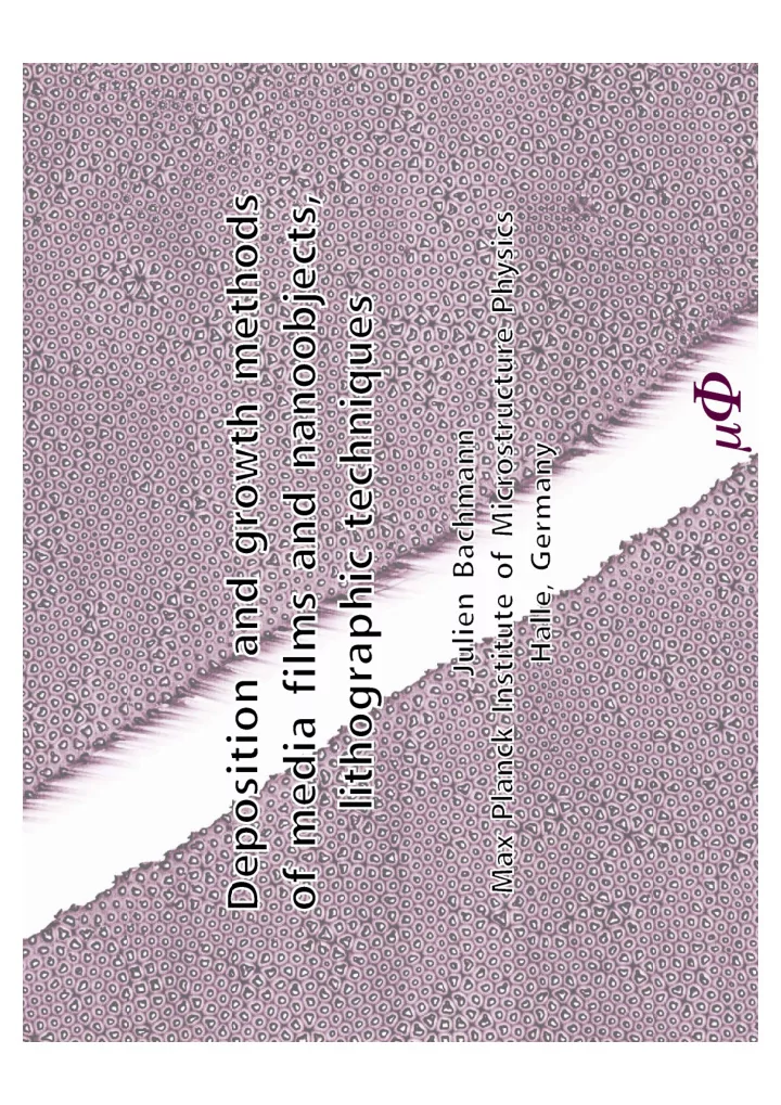
High-density data storage: principle Current approach High density - PDF document
High-density data storage: principle Current approach High density 1 bit = many domains 1 bit = 1 magnetic nanoobject Information storage driven Single-domain needed by domain wall shifts Single easy axis preferred Hurdle:
High-density data storage: principle Current approach High density 1 bit = many domains 1 bit = 1 magnetic nanoobject Information storage driven Single-domain needed by domain wall shifts Single easy axis preferred Hurdle: superparamagnetism
Preparative methods for thin films • Thermal evaporation • Sputtering • Chemical vapor deposition (CVD) • Pulsed laser deposition (PLD) • Molecular beam epitaxy (MBE) For a review of physical vapor deposition techniques: Reichelt, Thin Solid Films 1990 , 191 , 91-126 • … Deposition rate limited by mass transfer of “precursor” from the gas phase Techniques only applicable to flat substrates �
High-density data storage: requirements Requirements Approaches a. A. Pseudo-1D magnetic Small lateral size high density objects (wires, tubes) � a , b b. � Ferromagnetism B. Lithography along preferred axis c information storage � � c. C. Ordered porous 2D organization information retrieval templates � A, c , d d. � Controlled geometry D. Electrodeposition and magnetism response foreseeable A � � and optimizable E. Atomic layer deposition A, d �
A Shape anisotropy 1D • Challenge for small objects: superparamagnetism (no ordering because not enough material) KV >> • Solution: set a single easy magnetization axis � kT K : magnetic anisotropy; V : volume; k : Boltzmann’s constant; T : temperature • Option 1: use magnetocrystalline anisotropy … difficulties:control of crystallinity and orientation, limitation in terms of materials • Option 2: pseudo- 1D-objects Magnetic phase diagram for a cube with uniaxial anisotropy Ross, Annu. Rev. Mater. Res. 2001 , 31 , 203-235
A Types of pseudo-1D objects 1D Rods, pillars Wires Limited shape anisotropy Most investigated Co pillars: Farhoud, J. Vac. Sci. Tech. B 1999 , 17 , Ni wires: Whitney, Science 1993 , 261 , 1316-131 3182-3185 Tubes Circles, disks, ellipses Few preparative methods > 1 bit per object ? Co / polymer tubes: Nielsch, J. Appl. Phys. 2005 , 98 , 034318 Au rings: Ji, Adv. Mat. 2006 , 18 , 2593-2596
B E-beam lithography, focused ion beam (FIB) litho • Principle: exposure of a sensitive layer to a tightly focused beam… its chemical identity changes upon exposure • Electron beam: electron microscopes provide a convenient source • FIB: ions are extracted under a high voltage from a liquid Ga droplet wetting a W tip, then mass-selected, collimated and focused • Advantage: versatility — large variety of structures can be designed in a computer and created just by proper control of the beam deflector • Disadvantage: not a parallel method — every object must be prepared individually Lithographic methods for magnetic nanostructures: Martin, J. Magn. Magn Mat. 2003 , 256 , 449-501
B Interference lithography litho • Interference btw two beams of monochromatic light creates a perfectly ordered periodic line pattern in photoresist: Farhoud, J. Vac. Sci. Tech. B 1999 , 17 , 3182-3185 • Double exposure yields circular or elliptical objects • Advantage: massively parallel
B Direct pattern transfer: etching litho • Reactive ion etching (RIE): plasma in a gas creates ions that are both highly reactive and (somewhat) specific • CHF 3 for SiO 2 O 2 for organic materials Cl 2 for Al 2 O 3 (Ar non-specific: ion milling) • The plasma is “above” etching occurs vertically � Ross, Annu. Rev. Mater. Res. 2001 , 31 , 203-235
B Indirect pattern transfer: mask litho • Patterned layer used as a mask for the deposition of magnetic material (sputtering, thermal evaporation, …) • Patterned layer then lifted off • Alternative: patterned layer is separated, then laid onto a photoresist and used as a shadow mask Ross, Annu. Rev. Mater. Res. 2001 , 31 , 203-235
B Indirect pattern transfer: imprint litho • Mechanical indentation of substrate with patterned “stamp”: Si Si Ni Ni Lee, Small 2006 , 2 , 978-982 • Soft lithography (using PDMS stamps) more practical see Xia, Annu. Rev. Mater. Sci. 1998 , 28 , 153-184; and Angew. Chem. Int. Ed. 1998 , 37 , 551-575
B Lithographic structures litho Ni pillars of two different diameters (H // z) Ross, Annu. Rev. Mater. Res. 2001 , 31 , 203-235 Limitation: aspect ratios accessible in “vertical” geometry
C Porous materials as templates template • An ordered array of vertical pores is the “ negative ” of an array of 1D objects. • If the pore array is tunable in geometry , then the wires / tubes obtained from it are as well. • The preparation of the porous material may be specific to a certain material system; but if the “filling method” is general, the quality of the template is transferred to the 1D objects in general � need to optimize geometric control once and for all !
C Ion track-etch filters template • Commercially available filters with pores of controlled diameter: from bombardment with nuclear fission fragments then chemical etch Martin, Science 1994 , 266 , 1961-1966 • Advantages: variety of pore diameters (<10 nm) available pore diameter homogeneous • Disadvantages: pores randomly scattered pores not parallel
C Phase-separated block copolymers template • Phase separation may lead to regular pattern; selective chemical etching then furnishes a porous template or a mask Park, Science 1997 , 276 , 1401- 1404 A, C: copolymer polystyrene / polybutadiene (PB removed by ozonation); B, D: etched pattern in Si 3 N 4
C Macroporous silicon template • Electrochemical oxidation of Si in HF solution under irradiation induces the formation and growth of pores • Pores are disordered unless lithographically pre- defined Grüning, Appl. Phys. Lett. 1996 , 6 , 747-749 Lehmann, J. Electrochem. Soc. 1993 , 140 , 2836-2843 • Limitation: pores rather large (>0.5 µm)
For references: C Anodic alumina Nielsch K , Nano Lett. 2002 , 2 , 677-680 template Masuda, Science 1995 , 266 , 1466-1468. • Electrochemical oxidation of Al in acidic solution induces the formation and growth of pores in Al 2 O 3 . Al � Al 3+ + 3 e – 2 Al 3+ + 3 H 2 O � Al 2 O 3 + 6 H + 2 H + + 2 e – � H 2 3– + 3 Al 2 O 3 + 6 H 2 X � AlX 3 H 2 O • Ordering depends on balance btw electron transfer processes and diffusion of water through the alumina barrier • Different conditions (acid, temperature, voltage) yield different geometries (20 nm < diameter < 200 nm) Scale bars: 100 nm
D Chemistry of electrodeposition electrodep • Electroplating solution: for example MX n / H y A / H 2 O M n+ : metal ion; X – : Cl – , ½ SO 4 2– , CN – , …; H y A: H 3 BO 3 , … • M n+ reduced at the cathode (working electrode, W ): M n+ + n e – M 0 � • At the anode (auxiliary electrode, A ): something must be oxidized (electrical circuit is closed, electrons cannot be created or destroyed)… 2 H 2 O – 4 e – O 2 + 4 H + � • HA and MX n make the solution electrically conductive (charges cannot accumulate) • To be avoided (or minimized): reduction of protons… 2 H + + 2 e – H 2 �
D Thermodynamics of electrodeposition electrodep • Some elements are harder to reduce than others… Mg 2+ + H 2 Mg + 2 H + –2.4 V � Fe 2+ + H 2 Fe + 2 H + –0.4 V � Pd 2+ + H 2 Pd + 2 H + +0.8 V � • List of thermodynamic properties of redox couples: table of standard reduction potentials • Arbitrary reference of the reduction potentials: H + / H 2 couple (could have been free e – in vacuum) • Practical aspects influencing potentials necessary for electrodeposition: concentrations, transport phenomena, surface tension effects
D Technique of electrodeposition electrodep • Deposition modes: DC galvanostatic (no control on thermodynamics) DC potentiostatic (thermodynamics set by turning a button) pulsed (better kinetic control: reactant delivery to electrode) • Proper setup: with reference electrode ( R ) … V applied btw R and W … i measured btw A and W • Two-electrode setup (no R ) often used in practice
D Electrodeposited nickel nanowires electrodep Nielsch, Appl. Phys. Lett. 2001 , 79 , 1360-1362 • Porous anodic alumina as template • Au layer sputtered on one side as electrode • DC or pulsed electrodeposition • Pores fill up with Ni from electrode … growth of Ni wires • Advantages: wires oriented diameter tunable SEM top view
D Segmented wires electrodep • Electrodeposition in porous template with alternation btw several different solutions: segments of several different metals • Length of segments defined by total time spent (total charge passed) in each solution Optical and electron micrographs of a (nonmagnetic) Ag / Au segmented wire Nicewarner-Peña, Science 2001 , 294 , 137-141
E Atomic layer deposition: idea ALD Chemical vapor deposition (CVD): • thermal decomposition on the substrate • diffusion rate-limiting… shadowing Atomic layer deposition (ALD): • limiting chemical reaction with excess reactant • layer-by-layer growth with arbitrary substrate geometry
E Atomic layer deposition: method ALD • Two alternatively pulsed precursors no reaction in the gas phase • Precursors thermally stable but reactive towards each other specific chemical reaction, no decomposition • Each precursor pulse = one chemisorbed monolayer no matter excess of precursor… conformal coating • Thickness proportional to number of ALD cycles independent of experimental conditions
Recommend
More recommend
Explore More Topics
Stay informed with curated content and fresh updates.
