FPGA%Timing%Models Many%FPGA%and%CPLD%vendors%provide%a% timing - PDF document
FPGA%Timing%Models Many%FPGA%and%CPLD%vendors%provide%a% timing model in%their%data%sheets%that%allow% estimation%of%path%delays. Some%example%path%delays%that%are%of%interest: Minimum%Pin%to%Pin%(combinational)%delay%
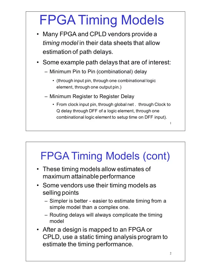
FPGA%Timing%Models • Many%FPGA%and%CPLD%vendors%provide%a% timing model in%their%data%sheets%that%allow% estimation%of%path%delays. • Some%example%path%delays%that%are%of%interest: – Minimum%Pin%to%Pin%(combinational)%delay% • (through%input%pin,%through%one%combinational%logic% element,%through%one%output%pin.) – Minimum%Register%to%Register%Delay% • From%clock%input%pin,%through%global%net%.%%through%Clock%to% Q%delay%through%DFF%of%a%logic%element,%through%one% combinational%logic%element%to%setup%time%on%DFF%input). 1 FPGA%Timing%Models%(cont) • These%timing%models%allow%estimates%of% maximum%attainable%performance • Some%vendors%use%their%timing%models%as% selling%points – Simpler%is%better%L easier%to%estimate%timing%from%a% simple%model%than%a%complex%one. – Routing%delays%will%always%complicate%the%timing% model • After%a%design%is%mapped%to%an%FPGA%or% CPLD,%use%a%static%timing%analysis%program%to% estimate%the%timing%performance. 2
Altera%M7000%Timing%Model 3 Altera%M7000%Timing%Defns 4
Altera%M7000E%Logic%Element 5 Actel%42MX%Timing%Model 6
Comb.%Pin%to%Pin%delay%Example Input-pad-through-combinational-element-through-output-pad From%timing%model: T INYL% +%%T IRD1 +%%T PD +%T RD1 +%%T DLH 1.16ns%+%2.24%ns%+%1.55ns%%%+%0.8%ns%+%2.7%ns Pin%to%Pin%=%%8.45%ns%% T INYL%%% Input%pad%to%Y%low T IRD1%% Input%Fanout%1%routing%delay%(higher%the%fanout,%longer% the%delay) T PD%%%%%%%%% Logic%module%prop%delay T RD1%%%%%% Output%Fanout%1%routing%delay T DLH%%%%%%% Data%to%Pad%high%delay 7 Environment%affects%Timing Actel-uses-derating-factors-for-timing-values.--A-derating-factor- is-a-multiplication-factor-applied-to-the-timing-value. Notice%that%fastest%timing%(smallest%derating%factor)%is%for% high%Voltage,%%low%temperature.%%The%slowest%timing% (largest%derating%factor)%is%for%low%voltage,%high% temperature.% Four%corners:%(low%temp,%low%Vdd),%(high%temp,%low% 8 Vdd),%(low%temp,%high%Vdd),%(high%temp,%high%Vdd).
Processing%Variations%can%also% affect%Timing Timing%can%vary%from%one%batch%of%wafers%to%another%due%to% process%variations.%%There%are%also% four-corners for% processing%variations:%(fastLp,%fastLn),%(slowLp,%fastLn),%(fastLp,% slowLn),%(slowLp,%slowLn).%%‘fastLp’,‘slowLp’%refer%to%fast%PMOS% transistors,%slow%PMOS%transistors.%%‘fastLn’,%‘slowLn’%refer%to% fast%NMOS%transistors,%slow%NMOS%transistors,%respectively. Data%sheets%use%timing%variations%due%to%processing%to% determine%the%speed%gradesa%%Voltage/Temperature%derating% factors%are%then%applied%to%individual%speed%grade%timings.%% Actel%specifies%a%0.45%derating%factor%for%best%case% processing.%This%would%be%important%if%you%were%trying%to% compute%the%minimum%delay.% 9 Speed%Grades • Important%to%realize%that%speed%grades%are% determined%via%the%timing%variations%due%to% processing – There%are%no%functional%differences%between% speed%grades. – A%functional%difference%would%require%a%different% part%number. • Vendors%will%charge%premium%prices%for%the% best%speed%grade%parts 10
Altera%IO%Element Logic% PIN Element% array 11 Altera%IOE%Timing%model Tiod Tiocomb Tod1 PIN Tincomb 12
IOE%(I/O%Element)% Delays • Input%path – Tincomb%L input%pad%and%buffer%to%fasttrack% interconnect%delay • Output%path%(combinational%path%with%fast% output%slew) – Tiod%%L data%delay – Tiocomb%L combinational%delay – Tod1%L slow%rate%=%off,%Vccio%=%Vccint%(Vcc%of%IO% pad%is%same%as%internal%Vcc). 13 Aside:%Why%programmable% Output%slew? • Slew%rate%is%the%measure%of%how%fast%an% output%can%change%value%(measured%in% Volts/Sec). • Most%FPGA%vendors%offer%the%capability%of% programming%the%output%to%be%either%fast%slew% or%slow%slew%LLLLL WHY? – Fast%Slew%rates%cause%more%noise%problems%via% ground%bounce,%especially%when%multiple%outputs% are%switching – If%you%have%room%in%your%timing%spec,%should%use% slow%slew%rate%if%possible 14
GND%Bounce Vdd Large%change%of%current%on%Vdd/Gnd%pins% (inrush%current)%due%to%multiple%outputs% changing%simultaneously%causes%induced% voltage%on%GND%plane: v(t) = L * di/dt Larger%the%inductance,%larger%the%change%in% current,%larger%the%induced%voltage. Chip Two%ways%to%reduce%Voltage: Reduce%Inductance%:%%More%Vdd/gnd%pins (inductance%in%parallel%reduces%total% inductance),%better%packaging%(different% packages%have%more/less%inductance%than% others).%% Flex%10K20%240%pin%package%has%19%Vdd%pins,% 18%Gnd%pins). GND Reduce di/dt : slower%slew%rate!!!! 15 Altera%Logic%Element 16
Altera%Logic%Element Tlut Tcomb 17 Minimum%Combinational%Pin%To% Pin%Delay [Input Pin delay] + [Logic Element Delay] + [Output Delay] [Tincomb] + [Tlut + Tcomb] + [Tiod + Tiocomb + Tod1] What%about%Routing%Delays?%%%Table%36%&%44%(in%data% book)%has%routing%delays. Tdin2data%L delay%from%dedicated%input%or%clock%to%LE% data Tsamecolumn%L delay%from%LE%output%to%IOE%in%same% column Tsamerow%L delay%from%LE%output%IOE%in%same%row 18
Minimum%Combinational%Pin%To% Pin%Delay [Input Pin delay] + [Routing] + [Logic Element Delay] + [Routing] + [Output Delay ] [Tincomb] + [Tdin2data] + [Tlut + Tcomb] + [Minimum (same col,row)] + [Tiod + Tiocomb + Tod1] [ 3.1 ] + [4.3] + [1.4 + 0.5] + min(0.9,3.6) + [ 1.3 +0.0 + 2.6] = 14.1 ns if%ignore%routing,%then%8.9%ns%( this%is%what%marketing% may%quote%in%datasheets ).% Note%that%same%column%routing%much%faster%than%row% routing%(hence%dedicated%carry%chains%run%in%column% routing). 19 Minimum%Clock%to%Register [Input Pin delay] + [Routing] + [Logic element clock-to-Q] + [Routing] + [Logic Element Delay] + [Routing] + [Logic Element Setup Time] Logic Element Dedicated Clkpin LUT Q Clkpin Routing DFF Routing LUT D Q DFF 20
Minimum%Clock%to%Register [Input Pin delay] + [Routing] + [Logic element clock-to-Q] + [Routing] + [Logic Element Setup Time] Logic Element Dedicated Clkpin LUT Q Clkpin Routing Tc + Tco DFF Routing Tdclk2le Tsamecol LUT D Q Tsu DFF 21 Dedicated%Inputs/Clock%Pins%vs%IOE%inputs A%dedicated%input%pin%or%dedicated%clock%pin%does%not%have% the%IOE%logic.%%The%input%timing%is%specified%as%routing%delay% only: IOE Input Routing Tincomb + Tsamecol = 3.1ns + 1.4ns = 4.4 ns Dedicated%Clkpin Use%dedicated%input%pins%to% minimize%input%delay.%%Not%% Clkpin Routing many%on%device%L 10K20%240% pin%package%only%has%4% dedicated%inputs%and%2% Tdclk2le = 2.6 ns dedicated%clock%pins. 22
Setup%Time%for%Logic%Element Tsu ? or LUT Tsu+Tlut? D Q DFF Typically,%the%setup%time%specification%for%an%external%data% input%already%accounts%for%the%LUT%delay%since%the%data% input%has%to%pass%through%the%LUT%on%its%way%to%the%D% input. The%Altera%spec%is%a%bit%confusing%L my%best%guess%is%that% Tsu%includes%the%LUT%delay.%%There%is%no%doubt%that%the% Xilinx%Virtex%Tsu%spec%includes%the%LUT%delay. 23 Clock%To%Out Two%different%Choices%here%L is%the%Dff%in%the%LUT%or%the%IOE?? Logic Element Dedicated Clock pin LUT Q Routing Routing Clkpin DFF IOE IOE Dedicated Clock pin Q Routing Output Clkpin DFF 24
Clock%To%Out Two%different%Choices%here%L is%the%Dff%in%the%LUT%or%the%IOE?? Logic Element Dedicated Clock pin LUT Tsamecol Q Routing Routing IOE Clkpin DFF Tc + Tco Tdclk2le Tiod + Tiocomb + Tod1 IOE Dedicated Clock pin DFF Q Routing Output Clkpin Tioc + Tioco + Tod1 Tdclk2ioe 25 Latching%in%I/O%Element%or%Logic% Element? • The%DFF%in%the%IOE%can%be%configured%to% either%latch%incoming%data%or%outgoing%data – Can%latch%ingoing/outgoing%data%in%either%IOE%or% LE%(logic%element) • Using%the%DFF%in%the%IOE%to%latch%outgoing% data%will%usually%reduce%ClockL2LOut%time – DFF%is%closer%to%the%Pin! • Using%the%DFF%in%the%IOE%to%latch%ingoing% data%will%reduce%external%setup%time. – DFF%is%closer%to%the%Pin! 26
Minimum%External%Setup%Time% Data%latched%in%LE IOE Input Routing LUT D Q Tsu_ext? Tsamecol Tsu Tincomb DFF Tsu_ext = Tincomb + Dedicated Clock pin Tsame col + Tsu - minimum(Tdclk2le) Routing Clkpin Tsu_ext = 3.1 ns + 1.4ns + Tdclk2le 1.3ns - 0 = 5.8 ns 27 Minimum%External%Setup%Time% Data%latched%in%%IOE IOE Tsu_ext = Tinreg + Tiosu Input D Q - minimum(Tdclk2le) Tsu_ext? Tinreg + Tiosu Tsu_ext = 6.0 ns + 2.8 - 0 = 8.8 ns Dedicated Clock pin !!%Latching%in%IOE%slower%than%in%Logic% Element?%%These%are%all%worse%case% numbers%in%the%datasheet%which%could% Routing account%for%thisa%also%mentioned%on%page%28% Clkpin that%latching%in%LE%element%will%sometimes% give%better%setup%time%than%an%IOE.%%%For% Tdclk2le other%FPGA%families%this%is%usually%not%the% case. 28
Chip%To%Chip Chip 1 IOE Dedicated Clock pin DFF Q Routing Output Clkpin Tioc + Tioco + Tod1 Tdclk2ioe Chip 2 IOE (clk2out + Tsu_ext) will be Q D constraint on how fast data is exchanged between chips Input Tinreg + Tiosu Tsu_ext 29 PLL%effects PLL/DLL%will%synchronize%internal%clock%to%external% clock.%%Aim%is%to%have%zero%delay%between%clock% edges%at%Logic%elements%and%external%clock%edge Dedicated Clock pin LUT Q Clk_ext Routing Clk_int Want%a%‘zeroLdelay’%clock,%%no%difference%in%edge% arrival%times%of%clock%edges%at%‘Clk_ext’%and% ‘Clk_int’. 30
Recommend
More recommend
Explore More Topics
Stay informed with curated content and fresh updates.


