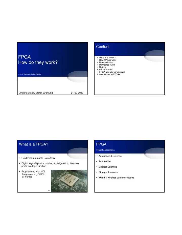

2/21/2012 Content FPGA • What is a FPGA? • How FPGAs work How do they work? • Manufacturers • Distributed RAM • History • FPGA vs ASIC • FPGA and Microprocessors • Alternatives to FPGAs ETI135, Advanced Digital IC Design Anders Skoog, Stefan Granlund 21-02-2012 What is a FPGA? FPGA Typical applications • Aerospace & Defense • Field-Programmable Gate Array • Automotive • Digital logic chips that can be reconfigured so that they preform a logic function preform a logic function • Medical/Scientific M di l/S i tifi • Programmed with HDL • Storage & servers languages e.g. VHDL or Verilog • Wired & wireless communications [B1] 1
2/21/2012 How FPGAs work How FPGAs work Cont FPGA Design • Block structure • CLB (Configureable Logic Block) • RAM • IOB • DSP • Microprocessors • Multipliers [B2] [B2] How FPGAs work How FPGAs work Cont Cont Logic-Cell Behaviour to duplicate Lookup on FPGA Smallest part in FPGA 3-input AND & OR Input Output 0000 0 0001 0 Consists at least of Consists at least of 0010 0 • Lookup Table (4-6 inputs) [B3] 0011 0 • D-flipflop 0100 0 0101 0 • MUX 0110 0 [B3] [B4] 0111 1 1000 1 1001 1 1010 1 1011 1 1100 1 1101 1 1110 1 1111 1 2
2/21/2012 How FPGAs work How FPGAs work Cont Cont Several Logic cells then gets interconnected [B5] [B7] [B6] How FPGAs work How FPGAs work Cont Cont Logic Cells can be connected to slices Interconnections between blocks is managed with Switch Matrices Several Slices form a CLB Several Slices form a CLB [B8] [B9] [B10] 3
2/21/2012 How FPGAs work How FPGAs work Cont Cont Interconnections between two adjacent CLB [B2] [B17] How FPGAs work How FPGAs work Cont Cont IOB [B2] [B14] 4
2/21/2012 How FPGAs work How FPGAs work Cont Cont Configuration of FPGA • The FPGA clears (initializes) the internal configuration memory • Configuration data is loaded into the internal memory • The user-application is activated by a start-up process [B18] How FPGAs work How FPGAs work Cont Cont Configuration of FPGA Example of VHDL-code [B4] [B11] 5
2/21/2012 Design Flow IP-Cores • IP-Cores are a reusable unit of logic, cell, or 1. Describe function in HDL or Schematic chip layout design that is the intellectual 2. Simulate property of one party. 3. Synthesize and create netlist 4 Simulate with netlist 4. Simulate with netlist • Soft cores: HDL code or as an Netlist S ft HDL d N tli t 5. Place and Route 6. Simulate/verify Place and Route • Hard cores: ASICs embedded on FPGA 7. Generate binary files 8. Upload to FPGA via JTAG interface or to a external memory • FFT, AC97, ARM processors, MIPS, MP3 device codec • Opencores.org Xilinx vs Altera Manufacturers Design philosophy Major manufacturers (80% of market): Xilinx: • Xilinx (over 50% of market) Tries to include as many features as possible, at the cost of • Altera increasing the complexity of the FPGA. Other manufacurers: Altera: • Lattice semiconductor Include the features most people use, to keep the complexity • Actel down. • SiliconBlue • QuickLogic ref. [1] 6
2/21/2012 Xilinx vs Altera Distributed RAM RAM-implementation • Xilinx and Altera use "big" RAM-blocks • Xilinx uses "Distributed RAM" for small RAMs • Xilinx patented technology • Altera mixes smaller and bigger blocks of RAM • Turns a Logic-cell in to a small 16bit RAM, ROM or ll 16bit RAM ROM FIFO shift register [B3] [B16] [B12] History History FPGA patent First commercially viable FPGA • XC2064 • Invented by Ross Freeman • 1985 • Patent filed in in 1984 describing basic FPGA functions • By co-founders of Xilinx Ross Freeman and Bernard B f d f Xili R F d B d Vonderschmitt “ Patent No. 4,870,302 -- Each configurable logic element in the array is in itself capable of performing any one of a plurality of • 64 CLB with two 3-input lookup tables logic functions depending upon the control information placed in the configurable logic element. Each configurable logic element • Today: Virtex 7 ~150 000 CLB with four 6-input lookup can have its function varied even after it is installed in a system by tables changing the control information placed in that element. “ Ref. [2] Ref. [2] [3] 7
2/21/2012 FPGA vs ASIC FPGA vs ASIC FPGA advantages ASIC advantages • Dynamic power: ASIC 12 x less than FPGA • Simpler design cycle • Area: ASIC 40 x less than FPGA • No "non recurring expenses" • Speed: ASIC 3.2 x faster than FPGA Speed: ASIC 3 2 x faster than FPGA • More predictable project cycle • Full custom capabillity • Reprogrammable • Lower unit cost • Shorter time to market, 9 months compared to 2 years Ref. [5] Ref. [4] FPGA vs ASIC FPGAs and Microprocessors What to choose? • Combining Serial and parallel processing ASIC • High volume products • Reconfiguring FPGA at "run-time" • Low power products • High speed • Loading firmware at Power on • Loading firmware at Power on FPGA • � Low to medium volume products • Needs to be flexible • Short development time [B13] 8
2/21/2012 FPGAs and Microprocessors CPLD Alternative to FPGA Hardware processor embedded in FPGA • PowerPC • Macocells with logic-gates and flip-flops • ARM Cortex-M3 • Non volatile configuration • Non-volatile configuration • Atmel memory Soft processor core • Constant signal delay • MicroBlaze • Not as flexible as FPGAs [B15] • Nios II • Less number of gates than a FPGA References Text [1] "Altera and Xilinx Report: The Battle Continues", 17-06-2008 http://seekingalpha.com/article/85478-altera-and-xilinx-report-the-battle-continues Thank you for listening [2] "Xilinx Co-Founder Ross Freeman Honored as 2009 National Inventors Hall of Fame Inductee for Invention of FPGA" , 11-02-2009 http://press.xilinx.com/phoenix.zhtml?c=212763&p=irol-newsArticle&ID=1255523&highlight [3] "FPGA Comparison Table", 17-02-2012, http://www.xilinx.com/products/silicon-devices/fpga/index.htm [4] Ian Kuon & Johnatan Rose "Measuring the Gap between FPGAs and ASICs" FPGA'06 February 2006 [4] Ian Kuon & Johnatan Rose, Measuring the Gap between FPGAs and ASICs , FPGA 06, February, 2006 http://www.eecg.toronto.edu/~jayar/pubs/kuon/kuonfpga06.pdf [5] Karthikeya "FPGA Vs ASIC Design: A Strategic Comparison" http://electronicsbus.com/fpga-vs-asic-design-verification-comparison/ [6] Spartan-3 Generation FPGA User Guide (v1.8), June 13, 2011 http://www.xilinx.com/support/documentation/user_guides/ug331.pdf Questions? [7] Spartan-3E FPGA Family Data Sheet (v3.8), August 26, 2009 http://www.xilinx.com/support/documentation/data_sheets/ds312.pdf 9
2/21/2012 References Pictures [B1] Anders Skoog, 16-02-2012 [B2] http://www.xilinx.com/company/gettingstarted/, Retrieved 19-02-2012 [B3] http://www.fpga4fun.com/FPGAinfo2.html , Retrieved 19-02-2012 [B4] Stefan Granlund, 20-02-2012 [B5] http://en.wikipedia.org/wiki/File:FPGA_cell_example.png, Peter källström, may 2010 [B6] Spartan-3E FPGA Family Data Sheet (v3.8), August 26, 2009, page 29 [B7] http://www.fpga4fun.com/FPGAinfo2.html , Retrieved 19-02-2012 [B8] Spartan-3 Generation FPGA User Guide (v1.8), June 13, 2011, page 396 [B9] Spartan-3 Generation FPGA User Guide (v1.8), June 13, 2011, page 396 [B10] Spartan 3E FPGA Family Data Sheet (v3 8) August 26 2009 page 22 [B10] Spartan-3E FPGA Family Data Sheet (v3.8), August 26, 2009, page 22 [B12] Xilinx Spartan-II FPGA Family Data sheet, 06-2008, page 3 [B11] Spartan-3E FPGA Family Data Sheet (v3.8), August 26, 2009, page 104 [B13] http://en.wikipedia.org/wiki/File:Xilinx_S6-SP601_board.jpg , CC-by-sa-3.0 licens , 19-02-201 [B14] Spartan-3E FPGA Family Data Sheet (v3.8), August 26, 2009, page 11 [B15] http://www.xilinx.com/company/gettingstarted/ , Retrieved 19-02-2012 [B16] Altera ACCEX 1K Data sheet ver. 3.4, may 2003, page 8 [B17] Spartan-3 Generation FPGA User Guide (v1.8), June 13, 2011, page 397 [B18] Spartan-3E Generation FPGA User Guide (v1.8), June 13, 2011, page 47 10
Recommend
More recommend