FPGA security Nele Mentens nele.mentens@kuleuven.be Design and - PDF document
FPGA security Nele Mentens nele.mentens@kuleuven.be Design and security of cryptographic algorithms and devices for real-world applications June 1-6, 2014, ibenik , Croatia Outline Introduction FPGA vs. ASIC FPGA application
FPGA security Nele Mentens nele.mentens@kuleuven.be Design and security of cryptographic algorithms and devices for real-world applications June 1-6, 2014, Šibenik , Croatia Outline • Introduction – FPGA vs. ASIC – FPGA application • FPGA technology – Architecture – Configuration – Design flow – Performance comparison • Crypto on FPGA – Area and speed optimization – AES design examples • Dynamic/partial reconfiguration Summer School, Šibenik , Croatia – June 1-6, 2014 1
Introduction FPGA vs. ASIC HW HW-SW SW General Domain DSP VLIW FPGA ASIC purpose specific Area efficiency Low High Performance/Energy unit Low High Programmability Summer School, Šibenik , Croatia – June 1-6, 2014 Introduction FPGA vs. ASIC • FPGA = Field-Programmable Gate Array • ASIC = Application-Specific Integrated Circuit • FPGA advantages over ASIC – faster time-to-market – smaller Non-Recurring Engineering (NRE) cost – programmable in the field • ASIC advantages over FPGA – lower cost for high volumes – better performance Summer School, Šibenik , Croatia – June 1-6, 2014 2
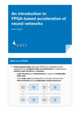
Introduction FPGA application • Prototype for ASIC design • End product – Recently developed FPGAs are heterogeneous systems with dedicated building blocks. – FPGAs closely follow technology scaling because they are manufactured in high volumes. • Application domains: – space – telecommunication – signal processing – … • Many applications require data security on FPGA. Summer School, Šibenik , Croatia – June 1-6, 2014 FPGA technology Architecture Basic FPGA architecture: • CLB = Configurable Logic Block – CLBs consist of slices. – Slices consist of • Look-Up Tables (LUTs), • Multiplexers, • Flip-Flops (FFs), • Carry logic. • SM = Switch Matrix • IOB = Input/Output Block Summer School, Šibenik , Croatia – June 1-6, 2014 3
FPGA technology Architecture basic content of a slice (excluding carry-logic) Look-Up Flip-Flop Table (FF) (LUT) Summer School, Šibenik , Croatia – June 1-6, 2014 FPGA technology Architecture basic principle of a switch matrix Summer School, Šibenik , Croatia – June 1-6, 2014 4
FPGA technology Architecture 1991: XC4000 configurable logic technology node: 0.25 µm Summer School, Šibenik , Croatia – June 1-6, 2014 FPGA technology Architecture 1991: XC4000 1998: Virtex block RAM block RAM configurable logic technology node: 0.22 µm Summer School, Šibenik , Croatia – June 1-6, 2014 5
FPGA technology Architecture 1991: XC4000 1998: Virtex 2002: Virtex-II Pro DCM DCM block RAM multipliers multipliers block RAM configurable logic rocket rocket IO IO power power PC PC technology node: 0.13 µm Summer School, Šibenik , Croatia – June 1-6, 2014 FPGA technology Architecture 1991: XC4000 1998: Virtex 2002: Virtex-II Pro 2004: Virtex-4 DCM DCM block RAM block RAM configurable DSP DSP logic rocket rocket IO IO power power PC PC technology node: 90 nm Summer School, Šibenik , Croatia – June 1-6, 2014 6
FPGA technology Architecture 1991: XC4000 1998: Virtex 2002: Virtex-II Pro 2004: Virtex-4 DCM DCM block RAM block RAM (PLL) (PLL) 2006: Virtex-5 DSP* configurable DSP* logic rocket rocket IO IO power power PC PC technology node: 65 nm Summer School, Šibenik , Croatia – June 1-6, 2014 FPGA technology Architecture 1991: XC4000 1998: Virtex 2002: Virtex-II Pro 2004: Virtex-4 DCM DCM block RAM block RAM (PLL) (PLL) DSP** 2006: Virtex-5 configurable DSP** logic 2009: Virtex-6 rocket rocket IO IO technology node: 45 nm Summer School, Šibenik , Croatia – June 1-6, 2014 7
FPGA technology Architecture 1991: XC4000 1998: Virtex 2002: Virtex-II Pro 2004: Virtex-4 DCM DCM block RAM block RAM (PLL) (PLL) DSP** 2006: Virtex-5 configurable DSP** logic 2009: Virtex-6 rocket rocket 2010: Virtex-7 IO IO ADC technology node: 28 nm Summer School, Šibenik , Croatia – June 1-6, 2014 FPGA technology Architecture • Latest development of Xilinx FPGAs: – Zynq-7000 series – ARM + FPGA – Processor-centered architecture Summer School, Šibenik , Croatia – June 1-6, 2014 8
FPGA technology Configuration • Configuration data: bitstream • Configuration technology: – (anti-)fuse: one-time programmable – flash: non-volatile configuration memory – SRAM: volatile configuration memory • SRAM (vs. flash) configuration memory – Higher density – Higher power consumption – On-board or on-chip non-volatile memory needed to store the bitstream during power-off – Higher configuration speed Summer School, Šibenik , Croatia – June 1-6, 2014 FPGA technology Configuration basic content of a slice (excluding carry logic) Look-Up Flip-Flop Table (FF) (LUT) Summer School, Šibenik , Croatia – June 1-6, 2014 9
FPGA technology Configuration basic content of a slice (excluding carry logic) + configuration Look-Up Flip-Flop Table (FF) (LUT) 1 configuration 16 configuration memory bits memory bit Summer School, Šibenik , Croatia – June 1-6, 2014 FPGA technology Configuration A B C D Z 0 Z 1 Z 2 Z 3 … Z 65280 … Z 65535 Why 16 configuration 0 0 0 0 0 1 0 1 0 1 bits for a 4-to-1 LUT? 0 0 0 1 0 0 1 1 0 1 0 0 1 0 0 0 0 0 0 1 2 16 possible output 0 0 1 1 0 0 0 0 0 1 functions: 0 1 0 0 0 0 0 0 0 1 0 1 0 1 0 0 0 0 0 1 Z 0 = 0 0 1 1 0 0 0 0 0 0 1 Z 1 = A’.B’.C’.D’ 0 1 1 1 0 0 0 0 0 1 Z 2 = A’.B’.C’.D 1 0 0 0 0 0 0 0 1 1 Z 3 = A’.B’.C’ 1 0 0 1 0 0 0 0 1 1 … 1 0 1 0 0 0 0 0 1 1 1 0 1 1 0 0 0 0 1 1 Z 65280 = A 1 1 0 0 0 0 0 0 1 1 … 1 1 0 1 0 0 0 0 1 1 Z 65535 = 1 1 1 1 0 0 0 0 0 1 1 1 1 1 1 0 0 0 0 1 1 Summer School, Šibenik , Croatia – June 1-6, 2014 10
FPGA technology Configuration basic principle of a switch matrix Summer School, Šibenik , Croatia – June 1-6, 2014 FPGA technology Configuration basic principle of a switch matrix + configuration = 1 bit configuration memory Summer School, Šibenik , Croatia – June 1-6, 2014 11
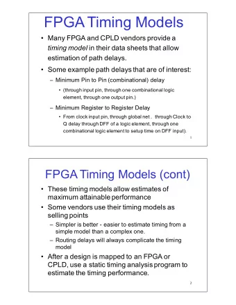
FPGA technology Design flow design entry schematic, VHDL, Verilog synthesis netlist implementation physical lay-out bitstream generation bitstream FPGA configuration Summer School, Šibenik , Croatia – June 1-6, 2014 FPGA technology Performance comparison • Be careful not to compare apples to oranges. • Performance depends on: – the place & route seed, – the degree of occupation, – the speed grade of the device. • Results from Saar Drimer’s Ph.D. dissertation Summer School, Šibenik , Croatia – June 1-6, 2014 12
Crypto on FPGA Area and speed optimization • Maximize the use of dedicated building blocks – Multipliers (in older FPGAs) • A*B • with or without registers – DSP slices (in more recently developed FPGAs) • version 1: A * B + C • version 2: (A + B) * C + D • many options for including or excluding pipeline registers – Block RAM • single-port or dual-port – Shift registers • a LUT can also be used as an addressable shift register Summer School, Šibenik , Croatia – June 1-6, 2014 Crypto on FPGA AES design examples Two examples: 1. P. Chodowiec, and K. Gaj , “Very Compact FPGA Implementation of the AES Algorithm”, C.D. Walter et al. (Eds.): CHES 2003, LNCS 2779, pp. 319 – 333, 2003. 2. S. Drimer, T. Güneysu, and C. Paar , “DSPs , BRAMs and a pinch of logic: extended recipes for AES on FPGAs”, ACM Transactions on Reconfigurable Technology and Systems (TRETS), 3(1), 2010. (pictures in the slides are copied from these publications) Summer School, Šibenik , Croatia – June 1-6, 2014 13
Crypto on FPGA AES design example 1 Encryption: addroundkey shiftrows, subbytes, mixcolumns, addroundkey (execute 9 times) shiftrows, subbytes, addroundkey Decryption: addroundkey invshiftrows, invsubbytes, addroundkey, invmixcolumns (execute 9 times) invshiftrows, invsubbytes, addroundkey Summer School, Šibenik , Croatia – June 1-6, 2014 Crypto on FPGA AES design example 1 Summer School, Šibenik , Croatia – June 1-6, 2014 14
Crypto on FPGA AES design example 1 Summer School, Šibenik , Croatia – June 1-6, 2014 Crypto on FPGA AES design example 1 Summer School, Šibenik , Croatia – June 1-6, 2014 15
Crypto on FPGA AES design example 1 Summer School, Šibenik , Croatia – June 1-6, 2014 Crypto on FPGA AES design example 2 round functions Summer School, Šibenik , Croatia – June 1-6, 2014 16
Crypto on FPGA AES design example 2 key schedule Summer School, Šibenik , Croatia – June 1-6, 2014 Dynamic/partial configuration • possible in SRAM-based FPGAs, • facilitates: – secure remote configuration, reconfigurable part: targeted application fixed part: comm + sec FPGA – IP core licensing, – implementation attack resistance. Summer School, Šibenik , Croatia – June 1-6, 2014 17
Recommend
More recommend
Explore More Topics
Stay informed with curated content and fresh updates.
