Australian Centre for Advanced Photovoltaics Fellow UNSW, Australia - PowerPoint PPT Presentation
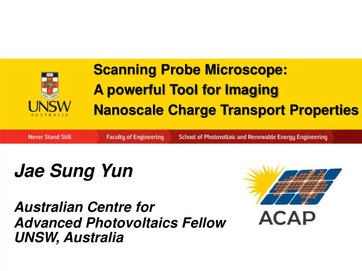
Scanning Probe Microscope: A powerful Tool for Imaging Nanoscale Charge Transport Properties Jae Sung Yun Australian Centre for Advanced Photovoltaics Fellow UNSW, Australia CONTENTS 1. Introduction to Scanning Probe Microscopy 2. Atomic Force
Scanning Probe Microscope: A powerful Tool for Imaging Nanoscale Charge Transport Properties Jae Sung Yun Australian Centre for Advanced Photovoltaics Fellow UNSW, Australia
CONTENTS 1. Introduction to Scanning Probe Microscopy 2. Atomic Force Microscopy 3. Kelvin Probe Force Microscopy 4. Contact Potential Difference 5. Surface Photovoltages 6. FAQ
MOTIVATION Crystalline Si thin film on Glass (CSG) Technology Any method to observe PV characteristics of structural defects in nanoscale? “Spatial resolution of few tenth of nanometre is J. Yun, et al. Appl. Phys. Lett. 2014 required”
ATOMIC FORCE MICROSCOPY “Atomic interaction between tip and the sample”
NON-CONTACT MODE AFM 1. Vibration at slightly above the resonance frequency of probe. 2. Rise to shift of the resonance frequency due to the interaction. 3. The changes in the oscillation amplitude are monitored and the feedback signals keeps constant the force gradient. Surface Science Reports 66 (2011) 1 – 27
KELVIN PROBE FORCE MICROSCOPY Przegląd Elektrotechniczny 91.9 (2015): 166- 169. 1st pass → Height Imaging height signal and CPD 2nd pass → CPD signal at the same spot!
CONTACT POTENTIAL DIFFERENCE (CPD) In equilibrium Before approach Nullifying voltage (CPD) through E v tunnelling Δ Ф = Ф t - Ф s Ф s Ф s V CPD = Ф t - Ф s E F Ф s Ф s Ф t Ф t Ф t E F Sample e e h h e e h h Sample Sample e e Tip Tip Tip h h e e h h e e An electrostatic force exists between tip and sample due to work function difference and DC voltage is applied to nullify the force. > 1 nm and >1 mV spatial resolution
CONTACT POTENTIAL DIFFERENCE (CPD) CPD measures work function of a sample surface Before passivation After passivation 500nm 500nm 500nm What does this mean to us? Advanced Energy Materials 8 (23), 1701940
CONTACT POTENTIAL DIFFERENCE (CPD) Narrower distribution Shift of work function Advanced Energy Materials 8 (23), 1701940 What made a shift of work function? - Charge carrier density, bandgap, surface states, surface dipole, crystal orientation It is always good to have results from other techniques such as SIMS, TEM, XRD, etc.
CONTACT POTENTIAL DIFFERENCE (CPD) Nature Communications 6, 7497 (2015) J. Yun et al. Advanced Energy Materials 6 (13), 1600330 Iodide vacancies in halide perovskite changes work function
ION MIGRATION IN HALIDE PEROVSKITE 0 V -7 V 1um 1um 4x4 µm J. Yun et al. Advanced Energy Materials 6 (13), 1600330 Grain boundaries are inflated due to the ion migration
ION MIGRATION IN HALIDE PEROVSKITE 500nm 500nm Grain boundaries act as channels for ion migration
DEGRDATION IN HALIDE PEROVSKITE J. Yun et al. Advanced Functional Materials 28 (3), 1705363 FAPbI3 Perovskite turn into non-perovskite phase at room temperature
DEGRDATION IN HALIDE PEROVSKITE Degradation time J. Yun et al. Advanced Functional Materials 28 (3), 1705363 Grains merge and grain boundaries become wide and lower CPD
DEGRDATION IN HALIDE PEROVSKITE Proposed Mechanism Moisture penetrate through the grain boundaries and yellow phase spreads laterally J. Yun et al. Advanced Functional Materials 28 (3), 1705363
OTHER APPLICATIONS Scientific reports 5 (2015): 8822 Philosophical magazine letters 85.1 (2005): 41-49.
SURFACE PHOTOVOLTAGE Surface photovoltage= CPD light -CPD dark n-type with majority carriers trapped at surface SPV can be expressed by the density of photogenerated charge carriers ( Δ n = Δ p) and the density of minority charge carriers in thermal equilibrium Top surface depleted by surface defects? Where is pn junction? What is bandgap? Lecture by Thoas Dittrich, HZB, 2010 What is diffusion length?
SURFACE PHOTOVOLTAGE Strong built-in potential Less trap states Transport layer Absorber TCO Intensity and wavelength dependent KPFM
SURFACE PHOTOVOLTAGE p-type vs n-type transport layer p-type n-type Every 40s
SURFACE PHOTOVOLTAGE 4.2 Contact Potential Difference as Function of Light Intensity J.Yun et al. The journal of physical chemistry letters 6 (5), 875-880 Sub-linear behavior of contact potential difference and open-circuit voltage Our obtained CPD can be correlated with the open circuit potential under illumination
GRAIN BOUNDARIES IN HALIDE PEROVSKITES CPD in Dark CPD in light Light Intensity Grain boundaries show higher CPD compare to grain interiors J.Yun et al. The journal of physical chemistry letters 6 (5), 875-880
PHOTOCURRENT MAPPING J.Yun et al. The journal of physical chemistry letters 6 (5), 875-880 Higher photocurrent at GBs
INORGANIC CATION INCORPORATED PEROVSKITES (FA x Rb 1−x PbI 3 ) 0.85 (MAPbBr 3 ) 0.15 ACS Energy Letters 2 (2), 438-444 Incoporation of Rb improved efficiency and stability
INORGANIC CATION INCORPORATED PEROVSKITES 500nm 500nm ACS Energy Letters 2 (2), 438-444 Cs and Rb forms nanoclusters and have higher SPV!!
LONG-CHAINED CATION MIXED PEROVSKITES ACS Energy Letters 3 (3), 647-654
LONG-CHAINED CATION MIXED PEROVSKITES Reference decrease in grain size 500nm 500nm 4.5%PEA Device Voc SPV ACS Energy Letters 3 (3), 647-654 Voc ↑ with grain size ↓ Enlarged bandgap at the GBs?
ALUMINA PASSIVATED CZTS SOLAR CELLS - negative charged interstitial O i Energy Environ. Sci. , 2019 Several nm thick Al 2 O 3 layer with trimethylaluminum (TMA) precursor enabled over 10% efficiency!
ALUMINA PASSIVATED CZTS SOLAR CELLS Energy Environ. Sci. , 2019 Higher response of CPD at both wavelengths when Al 2 O 3 is deposited on top of CZTS
CPD UNDER ILLUMINATION CPD UNDER ILLUMINATION 1um Grain to grain band gap difference from halide segregation 1um
CROSS-SECTION KPFM Nature communications 6 (2015): 7745. pn junction profile, charge transport properties at each interface, and band alignment
SUMMARY Allows 3D nanoscale mapping of your material! Work function distribution, ion migration, charge transport, surface photovoltage, pn junction properties, and many more!
WHERE IS AFM? SPREE- Park System School of Materials Science NX10 Several AFMs Prof. Jan Seidel Humidity control, different To be installed soon! environments, temperature control, KPFM with LED lights, conductive AFM, local tuneable laser, liquid IV curve, EFM, PFM, Phase imaging
FAQS 1. How long does it take to measure? For instances, 5 x 5 um 2 ? 2. How easy is it obtain a high quality CPD image? 3. What type of probe to use? 4. What sample roughness is allowed? Height CP D
Acknowledgement Special thanks to: Martin Green (UNSW) Jan Seidel (UNSW) Thanks to my collaborators: Sang Il Seok (UNIST) Jincheol Kim (KETI) Thanks to Dohyung Kim (Tennessee Ziv, Jessica, Ned, Jeana, University) Shujuan, Jun Hong Noh (Korea University) Jeana Hao (UNSW) Stephen for their Anita Ho-Baillie (UNSW) contribution! Shujuan Huang (UNSW) Of course, SPREE and SPREE Jangwon Seo (KRICT) people! Jung Ho Yun (UQ) And many others
Recommend
More recommend
Explore More Topics
Stay informed with curated content and fresh updates.
