Organic-Inorganic Hybrid Materials for IR-Photodetection and - PowerPoint PPT Presentation
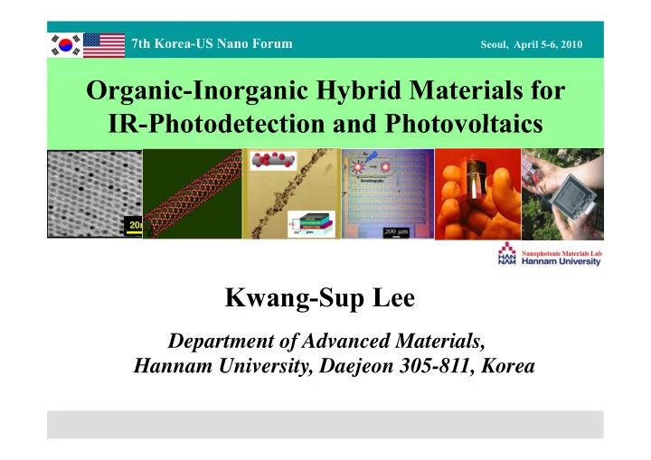
7th Korea-US Nano Forum Seoul, April 5-6, 2010 Organic-Inorganic Hybrid Materials for IR-Photodetection and Photovoltaics IR-Photodetection and Photovoltaics 20nm Kwang-Sup Lee D Department of Advanced Materials, f Ad d M i l Hannam
7th Korea-US Nano Forum Seoul, April 5-6, 2010 Organic-Inorganic Hybrid Materials for IR-Photodetection and Photovoltaics IR-Photodetection and Photovoltaics 20nm Kwang-Sup Lee D Department of Advanced Materials, f Ad d M i l Hannam University, Daejeon 305-811, Korea
Contents - Introduction I d i - Quantum Dot-based Hybrids Quantum Dot based Hybrids * Enhancing the Photocurrent Density * Photopatternable Quantum Dots * Photopatternable Quantum Dots - Low Bandgap Polymers Low Bandgap Polymers - C60 Derivatives - Summary
IR Photodetection Increase detectivity � Increase number of applications Medical Medical W Weather h Military (Thermal Imaging) Astronomy: Infrared Image of the Milky Way y y
Solar Spectrum
(Nanocrystal Quantum Dots) Pb (Lead) Se (Selenium ) Se (Selenium ) PbSe (for IR) CdSe, InP, InP-CdS core-shell (for visible) ZnSe, CdS (for UV) Z S CdS (f UV) • Semiconducting characteristics • Excellent quantum size effects • Excellent quantum size effects • Efficient excitonic generation • Tunable absorption and emission in Tunable absorption and emission in the UV to IR
Tuning of Spectral Response by Choosing Quantum Dots Absorption Luminescence ZnSe λ Broadband Absorber CdSe, InP CdSe, InP Quantum Dots λ PbSe λ CdSe QD 20n m
Preparation of PbSe Nanocrystals Ar organic capping to organic capping to precursors enable dispersion enable dispersion Thermocouple Heating mantle mantle Semiconductor quantum dot Stir plate reactants + core-shell/bipods/tripods/ tetrapods solvent (PbO + Oleic acid in tri n octylamine solvent)+ TOP Se or TBP Se (PbO + Oleic acid in tri- n -octylamine solvent)+ TOP-Se or TBP-Se Comments: Size and shape control + Surface functionalization of the particles are very important steps. ti l i t t t
Comparative Environmental Stabilities of IR QDs and IR Organic Dyes IR Organic Dyes Excitation - 720 nm Emission - 830 nm. Normal laboratory environmental storage environmental storage conditions.
Hybrid Materials for IR Photodetection QD / Pentacene / PVK Polymeric Nanocomposite Polymeric Nanocomposite Pentacene Pentacene
Synthetic Route for Pentacene Precursor Ali Afzali, et.al, J. Am. Chem. Soc . 2002 , 124 , 8812. O + H 3 C C N S O N -sulfinylacetamide y Pentacene Pentacene O N O CH 3 ReO 3 S CHCl 3 Pentacene precursor “ Soluble in CHCl 3 , CH 2 Cl 2 ” Prepared by the Diels-Alder reaction between pentacene & N-sulfinylamide in the presence of a catalytic amount of methyltrioxorhenium,
Device Processing for IR Photodetector O N n n O S N Pentacene precursor PbSe nanoparticle PVK PVK-Pentacene precursor-PbSe Film Baked in vacuum oven at 240 o C Measured Photoconductivity Film Composition: PVK 30 wt%, Pentacene precursor 30 wt%, PbSe 40 wt%
Evaluation of Photoconductivity sample sample ITO ITO ITO ITO electrode electrode focused focused light light collimated collimated R HV V Typical I-V Curve Keithley Keithley source meter source meter
Photocurrent density as a function of applied voltage in devices with the same proportion of PVK: pentacene (3:1) but various amounts of PbSe same proportion of PVK: pentacene (3:1) but various amounts of PbSe nanocrystals as indicated in the legend . Appl. Phys. Lett., 87, 051109 (2006) / US Patent 0128021 A1, 2008
Photocurrent density as a function of applied bias (1340 nm) in different devices with varying proportions of PVK and pentacene The photocurrent increases significantly as the amount of pentacene in the composite increases The photocurrent increases significantly as the amount of pentacene in the composite increases. The best performance was extracted in devices with equal amounts of PVK and pentacene (having 25 wt % of PbSe QDs). The enhancement in photocurrent, compared to a PVK-PbSe film, is over 8 times.
Comparison of the external quantum efficiency of the composite devices 2 25 wt % of PbSe % f S Max EQE: Max EQE: ~ 8% in the IR ~ 8% in the IR A maximum external quantum efficiency (EQE) of ~8% at an applied device bias of 5 V is achieved in the composite having equal amounts of PVK and pentacene. This is an improvement of eight times over the PVK:PbSe devices under similar experimental improvement of eight times over the PVK:PbSe devices under similar experimental conditions.
QD-Carbon Nanotube / PVK Polymeric Nanocomposite
Carbon Nanotubes Coupled with Quantum Dots SWCNT PbS QD SWCNT-PbSe QDs
SWCNT-CdSe SWCNT CdS SWCNT-CdS J. M. Haremza et al, Nano Lett. 2, 1253 (2002) SWCNT-CdSe I. Robel et al, Adv. Mater. 17, 2458 (2005) S. Banerjee et al, Nano Lett. 2, 195 (2002)
QD-SWCNT-Polymer Nanocomposites for Photovoltaics Photovoltaics Spacer: Aminoethanethiol: AET S A i h hi l AET NH 2 H 2 N NH 2 AET SH HS SH H 2 N QD QD HS SH ligand NH NH 2 SH HS SH H 2 N exchange NH 2 NH 2 COOH COOH COOH COOH carboxylation SWCNT COOH COOH COOH COOH Dots A variety of QDs active from UV to IR enables us to access a wide part of the solar spectrum
10 nm 10 nm 3 nm b
2500 2000 sity (a.u.) 1500 PL intens 1000 500 0 0 1000 1100 1200 1300 1400 1500 1600 Wavelength (nm) PL spectra of PbSe QDs (solid line) and SWNT-PbSe (dotted line) in tetracholoethylene colloidal suspensions. The concentration of y p PbSe QDs was the same in both cases.
I - V Characteristics of PbSe QD/PVK and SWNT-PbSe /PVK Device in Dark and under Illumination R H V V Keithley source meter Keithley source meter b Adv. Mater., 19, 232-236 (2007) / US Patent 2010-0025662 A1, 2011 ACS “Heart Cut” Research Highlight, 2007
Contents - Introduction I d i - Quantum Dot-based Hybrids Quantum Dot based Hybrids * Enhancing the Photocurrent Density * Photopatternable Quantum Dots * Photopatternable Quantum Dots - Low Bandgap Polymers Low Bandgap Polymers - C60 Derivatives - Summary
Surface Functionalization for Photo-Patternable QDs Chemical Amplification Reaction O O NH hv with H + catralyst hv with H + catralyst NH 2 D D O O O NH O H 2 N O S NH S NH 2 S S S Q S H QD O O N H 2 N S Δ S S S N O NH 2 O H S S S S S S HN HN S S H 2 N O HN O NH 2 O e O HN H 2 N O O S b P Nano Lett ., 8, 3262(2008 )
Photocurrent Measurements of Photopatternable QDs 5 CdTe (t-BOC protected) (a) 4 CdTe (Deprotected) ( p ) Dark rent (nA) 3 2 2 Curr 1 0 0 5 10 15 20 25 30 35 (b) Electric Field (MV/m) Current-voltage curves (a) in the dark or with white light (100 mW/cm 2 ) illumination for a film of t -BOC protected and deprotected CdTe nanocrystals (measured at the voltage scan rate is 1 V/s). The channel length is 5 μ m. MSM device structure (b) for photoconductivity measurement.
Polymer Nanocomposite Photovoltaics utilizing CdSe QDs Capped with a Thermally Cleavable Solubilizing Ligand Al P3HT: CdS P3HT: CdSe-amine i PEDOT ITO 1.5 Solar Cell Device Structure 2 ) nsity (mA/cm 1 2 ) /cm 1.0 0.1 Current den 0.01 0 01 sity (mA/ 0.5 1E-3 0.0 0.2 0.4 0.6 0.8 1.0 Voltage (V) 0.0 rent dens Thermal cleavage of -0.5 t-BOC o C (photo) 100 o C (dark) 100 100 C (dark) Curr -1.0 1 0 o C (photo) 200 o C (dark) 200 -1.5 0.0 0.2 0.4 0.6 0.8 1.0 Voltage (V) Appl. Phys. Lett., 94, 133302 (2009 )
O O O O O O Si O O Si Si S 11 O O S O 11 O Si O CdSe S O 11 S O Si 11 11 O O QD 1 UV: 552nm PL: 568nm
3-D Lithographic Microfabrication ♦ Localized photochemistry by TPA process C Collimated Laser Beam i Polymerized Polymerized region Photocurable film Focused beam Objective lens j Single-photon Two-photon polymerization polymerization Lens Lens TPA : volume of order λ 3 TPA : volume of order λ DOF Localized photo- polymerization polymerization Width Use of longer radiation wavelengths in TPA process is possible to achieve the better Use o o ge ad at o wave e gt s p ocess s poss b e to ac eve t e bette penetration depth in the medium
S PE Flu PV DTT S S S S R R R R R R S R OC 12 H 25 R R R R R OC 12 H 25 S S N N C 12 H 25 O C 12 H 25 O R R R R R R N N R R NBu2-DTTPE-NBu2 NBu2-DTTPE-NBu2 R R R R R R Polymers Ceramics Metals Metals
CdSe/ZnS Core-Shell CdSe Figure (a) shows the photocuring of working acrylate functionalized quantum dots with its layer structure, (b) Shows the synthesis scheme for the acrylate functionalized photopatternable quantum dots.
Photopatterns by Using CdSe/ZnS Core-Shell QDs Clli C o llim a t dL ted L a ser B B ea m Polymerized Polymerized region Photocurable film Size distribution of Nanorods: 10 -30 nm Focused beam Objective lens Single-photon Two-photon polymerization polymerization L L en s er λ 3 T P A : v o lu m e o f o rd D O F L L o o ca ca lizedp lized p h h o o to to - p o ly m eriza tio n W id th
Recommend
More recommend
Explore More Topics
Stay informed with curated content and fresh updates.
