Adv. Mater. 2014, 26, 30883093, (DOI: 10.1002/adma.201305457) - PowerPoint PPT Presentation
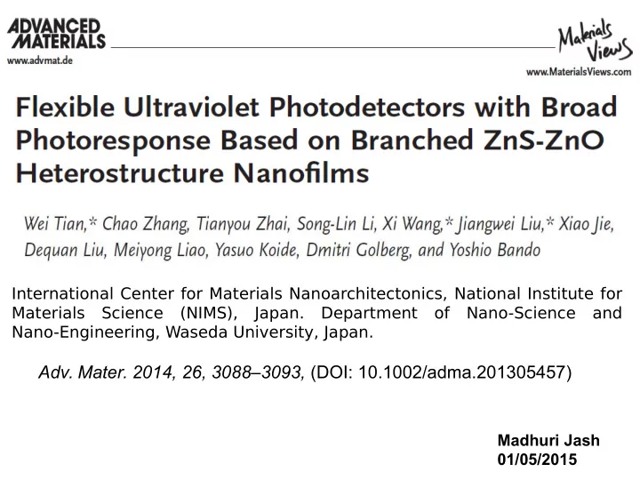
International Center for Materials Nanoarchitectonics, National Institute for Materials Science (NIMS), Japan. Department of Nano-Science and Nano-Engineering, Waseda University, Japan. Adv. Mater. 2014, 26, 30883093, (DOI:
International Center for Materials Nanoarchitectonics, National Institute for Materials Science (NIMS), Japan. Department of Nano-Science and Nano-Engineering, Waseda University, Japan. Adv. Mater. 2014, 26, 3088–3093, (DOI: 10.1002/adma.201305457) Madhuri Jash 01/05/2015
INTRODUCTION: One dimentional nano/heterostructures service as building blocks which play a key role to tailor some specifjc properties in nanoelectronic and optoelectronic devices. Particularly branched heterostructures consisting of two components exhibit unique and enhanced performances. ZnO and ZnS are semiconductors with band-gaps of 3.37 and 3.67 eV respectively, have been studied as visible-blind UV photodetectors. However as the UV light photodetector, ZnS nanostructures show weak photocurrent and less stability. Again ZnO nanostructures have a slow response and poor photocurrent stability due to natural defects. But it also should be noted that ZnS based photodetectors have fast response and ZnO has good contacts with electrodes and possess large photocurrent.
In this paper…….. So, in this paper they have combined the unique properties of individuals constituents. They have prepared hybrid ZnS-ZnO nanostructures including high sensitivity, fast response speed and broad UV range photoresponse.
SYNTHETIC PROCEDURE: So here they have prepared branched ZnS-ZnO nanostructures by combining a facile thermal evaporation process and a hydrothermal growth. ZnS nanowires were prepared by thermal evaporation method by using ZnS powder as the source material in a tube furnace at 1000 C. Then ZnS nanowires were coated with ZnO nanoparticles by a dip-coating method. After that hydrothermal process was conducted at 95 C for 8 h and then substrates were removed and washed with deionized water followed by drying in an Ar flow.
CHARACTERIZATION: Fig:1 a) X-ray diffraction (XRD) patterns of primary ZnS nanowires and branched ZnS-ZnO heterostructures. b) Room temperature PL spectra of the ZnS nanowires and branched heterostructures measured in a spectral range of 325–800 nm.
Fig: 2 c, d)SEM images of ZnS nanowires. e, f) SEM images of the branched heterostructures.
Fig: 3 a) HRTEM image of a ZnS nanowire. The inset is the corresponding FFT pattern. b) Typical TEM image of an individual ZnS-ZnO branched nanostructure. c) HRTEM image of a ZnS-ZnO branched nanostructure. d) The interface between ZnS and ZnO phases.
DEVICE MEASUREMENTS: Fig: 4 Schematic illustration of nanowire film transfer onto PET substrate and an overall device structure Fig: 5 Spectroscopic photoresponses of a) ZnS and b) ZnS-ZnO devices measured at a bias of 5.0 V at different wavelengths ranging from 250 to 630 nm. The inset is the optical absorption spectrum.
Fig: 6 c) I–V curves of the ZnS-ZnO device. d) I–V curves of the device illuminated at 320 nm wavelength. e) Time-dependent response of the device measured in vacuum conditions at a bias of 10.0 V. f) I–V curves of the device at initial stage, after 200 cycles of bending and stored in air for two Months.
Fig: 7 a) An optical image of the ZnS-ZnO devices on a PET substrate and micrographs of three as-fabricated devices. b, c) I–V curves under 320 nm light illumination in air and vacuum for all measured devices. d) The bar chart of the photocurrent in air and vacuum for all measured devices.
CONCLUSIONS: So, they have developed a novel nanofilm-based photodetectors from ZnS-ZnO branched nanostructures. The photodetectors exhibit high spectral selectivity and wide-range photoresponse for UV light. The optimized performance of this hybrid photodetector is much better than that of pure ZnS or ZnO nanostructures. Again this technique is an attractive alternative to standard semiconductor processing techniques. It have a great potential as optoelectronic and photoelectronic switches.
FUTURE DIRECTIONS…….. Can we combine the electrospinning and electrospray to form this type of structure which can acts as a sensor ?
THANK YOU
Recommend
More recommend
Explore More Topics
Stay informed with curated content and fresh updates.




![arXiv:1002.4546v1 [math.PR] 24 Feb 2010 Nonlinear Expectations and Stochastic Calculus under](https://c.sambuz.com/145197/arxiv-1002-4546v1-math-pr-24-feb-2010-s.webp)


