Electrical modeling of the photoelectric effect induced by a pulsed - PowerPoint PPT Presentation
Electrical modeling of the photoelectric effect induced by a pulsed laser applied to an SRAM cell. A. Sarafianos a,b , C. Roscian b , J.M. Dutertre b , M. Lisart a , A. Tria b . a STMicroelectronics, Avenue Clestin Coq 13790 Rousset, France b
Electrical modeling of the photoelectric effect induced by a pulsed laser applied to an SRAM cell. A. Sarafianos a,b , C. Roscian b , J.M. Dutertre b , M. Lisart a , A. Tria b . a STMicroelectronics, Avenue Célestin Coq 13790 Rousset, France b Centre de Microélectronique de Provence - Georges Charpak 880 Avenue de Mimet 13541 Gardanne, France
Outline Page Introduction 3 Electrical modeling of PN junctions under PLS 5 Presentation of the SRAM cell 7 Theoretical sensitive areas 8 Laser characterization of the SRAM cell 9 Hypothesis 10 SEU sensitivity simulation of the SRAM cell 11 Conclusion 15 2
Introduction 1/2 Radiation emitted from the Effect of radiation could be tested by: sun is a major threat for Cyclotron or Pulsed Laser equipment electronics devices Possible simulation: TCAD Electrical simulation 3
Introduction 2/2 Characterization and modeling of CMOS devices under laser illumination N+/Psub P+/Nwell Nwell/Psub Confirm the simplify model on CMOS gate: + = e.g.: inverter, SRAM cell… A. Sarafianos and al, Building the electrical model of the A. Sarafianos and al, Building the electrical model of the pulsed photoelectric laser stimulation of a PMOS pulsed photoelectric laser stimulation of an NMOS transistor in 90nm technology, IPFA 2013. transistor in 90nm technology, IRPS 2013. 4
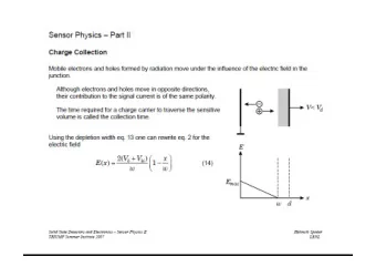
Electrical modeling of photocurrents (Iph) induced in PN junctions Sub circuit for each kind of PN junction Nwell P+ N+ Iph Iph Iph V V V Nwell Psub Psub 5
Electrical modeling of photocurrents (Iph) induced in PN junctions Sub circuit for each kind of PN junction Nwell P+ N+ Junction area Reverse biased voltage Iph Iph Iph V V V Nwell Psub Psub Trig signal Dependency of the pulse width Takes into account spatial dependency 6
Measurement vs electrical simulation for PN junctions under pulsed laser illumination N+/Psub P+/Nwell Good correlation obtain between measurement and electrical simulation permits to build an electrical model of PN junctions under pulsed laser illumination 7
Presentation of the SRAM cell CSRAM 5T Convention: State “0” DATA_OUT = “0” State “1” DATA_OUT = “1” 8
Theoretical sensitive areas 4 sensitive areas in theory 2 in state “0” • Drain of MP1 • Drain of MN2 And 2 others in state “1” • Drain of MP2 • Drain of MN1 9
Laser characterization of the SRAM cell Laser equipment features Wavelength 1064 nm Spot size 1 µ m Pulse duration 50 ns Laser power 1.7W Only 3 sensitive areas revealed by measurement 2 in state “0” • Drain of MP1 • Drain of MN2 And 1 others in state “1” • Drain of MP2 10
Hypothesis In state 1 Schematic 4µm 9µm 11
Hypothesis In state 1 Schematic 4µm 9µm 12
Hypothesis In state 1 Schematic 4µm 9µm near Large area of Small area of Masking effect the Drain of the Drain of MN2/MN3 MP2 13
Electrical modeling of the SRAM and results Electrical modeling Electrical simulation result Comparison with measurement A C B 14
Waveforms on point A Modification of the state of the SRAM from 0 to 1 A 15
Waveforms on point B Modification of the state of the SRAM from 1 to 0 B 16
Waveforms on point C No state modification C 17
Conclusion ◙ Simulation permits to validate the hypothesis of masking effect. The topology of the cell has an important effect! ◙ The validity of our modeling approach is assessed by the good correlation obtained between simulations and measurements. ◙ Perspectives: Simulate new solution more robust against laser injection. 18
Thank you for your attention… Q & A 19
Recommend
More recommend
Explore More Topics
Stay informed with curated content and fresh updates.
