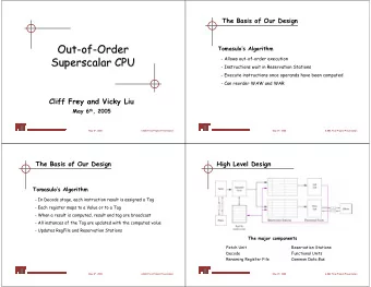
A Superscalar Out-of-Order x86 Soft Processor for FPGA Henry Wong - PowerPoint PPT Presentation
A Superscalar Out-of-Order x86 Soft Processor for FPGA Henry Wong University of Toronto, Intel henry@stufgedcow.net June 5, 2019 Stanford University EE380 1 Hi! CPU architect, Intel Hillsboro Ph.D., University of Toronto Today:
Processor Area and Frequency Component Estimated Frequency Area (ALM) (MHz) Decode * 6 000 247 Renaming 1 900 317 Scheduler * 4 000 275 Register fjle 2 400 260 Execution 2 300 240 Memory system (Logic) 9 000 200 (Caches) 5 000 Commit + ROB * 2 000 Microcode * 500 Total 28 700 200 * Area estimate for partial or unimplemented circuit ● Compare to Nios II/f with MMU and 32K L1I + 32K L1D – 4400 ALM (6.5× ), 245 MHz (0.82× ) 36
Processor Area and Frequency Component Estimated Frequency Area (ALM) (MHz) Decode * 6 000 247 Renaming 1 900 317 Scheduler * 4 000 275 Register fjle 2 400 260 Execution 2 300 240 Memory system (Logic) 9 000 200 (Caches) 5 000 Commit + ROB * 2 000 Microcode * 500 Total 28 700 200 * Area estimate for partial or unimplemented circuit 7% of Stratix IV ● Compare to Nios II/f with MMU and 32K L1I + 32K L1D – 4400 ALM (6.5× ), 245 MHz (0.82× ) 37
Processor Area and Frequency Component Estimated Frequency Area (ALM) (MHz) Decode * 6 000 247 Renaming 1 900 317 Scheduler * 4 000 275 Register fjle 2 400 260 Execution 2 300 240 Memory system (Logic) 9 000 200 (Caches) 5 000 Commit + ROB * 2 000 Optimize more? Microcode * 500 Total 28 700 200 * Area estimate for partial or unimplemented circuit 7% of Stratix IV ● Compare to Nios II/f with MMU and 32K L1I + 32K L1D – 4400 ALM (6.5× ), 245 MHz (0.82× ) 38
Processor Area and Frequency Component Estimated Frequency Area (ALM) (MHz) Decode * 6 000 247 Renaming 1 900 317 Scheduler * 4 000 275 Register fjle 2 400 260 “OoO stufg” Execution 2 300 240 Memory system (Logic) 9 000 200 (Caches) 5 000 Commit + ROB * 2 000 Optimize more? Microcode * 500 Total 28 700 200 * Area estimate for partial or unimplemented circuit 7% of Stratix IV ● Compare to Nios II/f with MMU and 32K L1I + 32K L1D – 4400 ALM (6.5× ), 245 MHz (0.82× ) 39
Per-clock performance (SPECint2000) Slower VIA C3 550 MHz 2.68 Nios II/f 100 MHz 2.73 2.06 Pentium 200 MHz Atom (Bonnell) 1600 MHz 1.63 1.46 AMD K6 166 MHz Pentium 4 2800 MHz 1.58 1.42 ARM Cortex-A9 800 MHz 1.26 Pentium Pro 233 MHz This work ~200 MHz 1.00 0.99 Atom (Silvermont) 2400 MHz VIA Nano 1000 MHz 0.87 0.91 Opteron K8 2800 MHz AMD Piledriver 3500 MHz 0.68 Core 2 Q9550 3400 MHz 0.56 0.44 Haswell 4300 MHz 0.0 0.5 1.0 1.5 2.0 2.5 3.0 Relative Runtime Cycles 40
Per-clock performance (SPECint2000) Slower ● Nios II/f: 2.73× VIA C3 550 MHz 2.68 Nios II/f 100 MHz 2.73 – Wall-clock: 2.23× 2.06 Pentium 200 MHz ● Pentium Pro (1995): 1.26× Atom (Bonnell) 1600 MHz 1.63 – Also 8 KB/256 KB cache 1.46 AMD K6 166 MHz – 3-way OoO Pentium 4 2800 MHz 1.58 ● Atom Silvermont (2013): 0.99× 1.42 ARM Cortex-A9 800 MHz 1.26 Pentium Pro 233 MHz – Also 2-way OoO This work ~200 MHz 1.00 – 32 KB/2 MB cache 0.99 Atom (Silvermont) 2400 MHz VIA Nano 1000 MHz 0.87 ● Large performance increases vs. Nios II/f 0.91 Opteron K8 2800 MHz AMD Piledriver 3500 MHz 0.68 ● Comparable per-clock performance to Core 2 Q9550 3400 MHz 0.56 similar x86 microarchitectures 0.44 Haswell 4300 MHz 0.0 0.5 1.0 1.5 2.0 2.5 3.0 Relative Runtime Cycles 41
Per-clock performance (SPECint2000) Slower ● Nios II/f: 2.73× VIA C3 550 MHz VIA C3 550 MHz 2.68 2.68 Nios II/f 100 MHz Nios II/f 100 MHz 2.73 2.73 – Wall-clock: 2.23× 2.06 2.06 Pentium 200 MHz Pentium 200 MHz ● Pentium Pro (1995): 1.26× Atom (Bonnell) 1600 MHz Atom (Bonnell) 1600 MHz 1.63 1.63 – Also 8 KB/256 KB cache 1.46 1.46 AMD K6 166 MHz AMD K6 166 MHz – 3-way OoO Pentium 4 2800 MHz Pentium 4 2800 MHz 1.58 1.58 ● Atom Silvermont (2013): 0.99× ARM Cortex-A9 800 MHz 1.42 1.42 ARM Cortex-A9 800 MHz 1.26 1.26 Pentium Pro 233 MHz Pentium Pro 233 MHz – Also 2-way OoO This work ~200 MHz This work ~200 MHz 1.00 1.00 – 32 KB/2 MB cache 0.99 0.99 Atom (Silvermont) 2400 MHz Atom (Silvermont) 2400 MHz VIA Nano 1000 MHz VIA Nano 1000 MHz 0.87 0.87 ● Large performance increases vs. Nios II/f Opteron K8 2800 MHz 0.91 0.91 Opteron K8 2800 MHz 0.68 AMD Piledriver 3500 MHz AMD Piledriver 3500 MHz 0.68 ● Comparable per-clock performance to Core 2 Q9550 3400 MHz Core 2 Q9550 3400 MHz 0.56 0.56 similar x86 microarchitectures 0.44 0.44 Haswell 4300 MHz Haswell 4300 MHz 0.0 0.0 0.5 0.5 1.0 1.0 1.5 1.5 2.0 2.0 2.5 2.5 3.0 3.0 Relative Runtime Cycles Relative Runtime Cycles 42
Per-clock performance (SPECint2000) Slower ● Nios II/f: 2.73× VIA C3 550 MHz VIA C3 550 MHz VIA C3 550 MHz 2.68 2.68 2.68 Nios II/f 100 MHz Nios II/f 100 MHz Nios II/f 100 MHz 2.73 2.73 2.73 – Wall-clock: 2.23× 2.06 2.06 2.06 Pentium 200 MHz Pentium 200 MHz Pentium 200 MHz ● Pentium Pro (1995): 1.26× Atom (Bonnell) 1600 MHz Atom (Bonnell) 1600 MHz Atom (Bonnell) 1600 MHz 1.63 1.63 1.63 – Also 8 KB/256 KB cache 1.46 1.46 1.46 AMD K6 166 MHz AMD K6 166 MHz AMD K6 166 MHz – 3-way OoO Pentium 4 2800 MHz Pentium 4 2800 MHz Pentium 4 2800 MHz 1.58 1.58 1.58 ● Atom Silvermont (2013): 0.99× ARM Cortex-A9 800 MHz ARM Cortex-A9 800 MHz 1.42 1.42 1.42 ARM Cortex-A9 800 MHz 1.26 1.26 1.26 Pentium Pro 233 MHz Pentium Pro 233 MHz Pentium Pro 233 MHz – Also 2-way OoO This work ~200 MHz This work ~200 MHz This work ~200 MHz 1.00 1.00 1.00 – 32 KB/2 MB cache 0.99 0.99 0.99 Atom (Silvermont) 2400 MHz Atom (Silvermont) 2400 MHz Atom (Silvermont) 2400 MHz VIA Nano 1000 MHz VIA Nano 1000 MHz VIA Nano 1000 MHz 0.87 0.87 0.87 ● Large performance increases vs. Nios II/f Opteron K8 2800 MHz Opteron K8 2800 MHz 0.91 0.91 0.91 Opteron K8 2800 MHz 0.68 0.68 AMD Piledriver 3500 MHz AMD Piledriver 3500 MHz AMD Piledriver 3500 MHz 0.68 ● Comparable per-clock performance to Core 2 Q9550 3400 MHz Core 2 Q9550 3400 MHz Core 2 Q9550 3400 MHz 0.56 0.56 0.56 similar x86 microarchitectures 0.44 0.44 0.44 Haswell 4300 MHz Haswell 4300 MHz Haswell 4300 MHz 0.0 0.0 0.0 0.5 0.5 0.5 1.0 1.0 1.0 1.5 1.5 1.5 2.0 2.0 2.0 2.5 2.5 2.5 3.0 3.0 3.0 Relative Runtime Cycles Relative Runtime Cycles Relative Runtime Cycles 43
Per-clock performance (SPECint2000) Slower ● Nios II/f: 2.73× VIA C3 550 MHz VIA C3 550 MHz VIA C3 550 MHz VIA C3 550 MHz 2.68 2.68 2.68 2.68 Nios II/f 100 MHz Nios II/f 100 MHz Nios II/f 100 MHz Nios II/f 100 MHz 2.73 2.73 2.73 2.73 – Wall-clock: 2.23× 2.06 2.06 2.06 2.06 Pentium 200 MHz Pentium 200 MHz Pentium 200 MHz Pentium 200 MHz ● Pentium Pro (1995): 1.26× Atom (Bonnell) 1600 MHz Atom (Bonnell) 1600 MHz Atom (Bonnell) 1600 MHz Atom (Bonnell) 1600 MHz 1.63 1.63 1.63 1.63 – Also 8 KB/256 KB cache 1.46 1.46 1.46 1.46 AMD K6 166 MHz AMD K6 166 MHz AMD K6 166 MHz AMD K6 166 MHz – 3-way OoO Pentium 4 2800 MHz Pentium 4 2800 MHz Pentium 4 2800 MHz Pentium 4 2800 MHz 1.58 1.58 1.58 1.58 ● Atom Silvermont (2013): 0.99× ARM Cortex-A9 800 MHz ARM Cortex-A9 800 MHz ARM Cortex-A9 800 MHz 1.42 1.42 1.42 1.42 ARM Cortex-A9 800 MHz 1.26 1.26 1.26 1.26 Pentium Pro 233 MHz Pentium Pro 233 MHz Pentium Pro 233 MHz Pentium Pro 233 MHz – Also 2-way OoO This work ~200 MHz This work ~200 MHz This work ~200 MHz This work ~200 MHz 1.00 1.00 1.00 1.00 – 32 KB/2 MB cache 0.99 0.99 0.99 0.99 Atom (Silvermont) 2400 MHz Atom (Silvermont) 2400 MHz Atom (Silvermont) 2400 MHz Atom (Silvermont) 2400 MHz VIA Nano 1000 MHz VIA Nano 1000 MHz VIA Nano 1000 MHz VIA Nano 1000 MHz 0.87 0.87 0.87 0.87 ● Large performance increases vs. Nios II/f Opteron K8 2800 MHz Opteron K8 2800 MHz Opteron K8 2800 MHz 0.91 0.91 0.91 0.91 Opteron K8 2800 MHz 0.68 0.68 0.68 AMD Piledriver 3500 MHz AMD Piledriver 3500 MHz AMD Piledriver 3500 MHz AMD Piledriver 3500 MHz 0.68 ● Comparable per-clock performance to Core 2 Q9550 3400 MHz Core 2 Q9550 3400 MHz Core 2 Q9550 3400 MHz Core 2 Q9550 3400 MHz 0.56 0.56 0.56 0.56 similar x86 microarchitectures 0.44 0.44 0.44 0.44 Haswell 4300 MHz Haswell 4300 MHz Haswell 4300 MHz Haswell 4300 MHz 0.0 0.0 0.0 0.0 0.5 0.5 0.5 0.5 1.0 1.0 1.0 1.0 1.5 1.5 1.5 1.5 2.0 2.0 2.0 2.0 2.5 2.5 2.5 2.5 3.0 3.0 3.0 3.0 Relative Runtime Cycles Relative Runtime Cycles Relative Runtime Cycles Relative Runtime Cycles 44
Summary 1 ● Designed microarchitecture and circuits for a superscalar out-of-order x86 soft processor – Both user and system modes ● Area: 6.5× Nios II/f, but afgordable – 7% Stratix IV or 1.3% Stratix 10 ● Performance: 2.2× Nios II/f on SPECint2000 – Per-clock: ~2.7× – Frequency: ~0.8× ● Out-of-order increases soft processor performance without rewriting software ● x86 is feasible on FPGA 45
Part 2: Pipeline Details ● Sketch of interesting circuits at each stage ● Timing budget: ~5 LUT levels (< 3.5 ns) ● Many circuits designed bottom-up – LUT granularity 46 Fetch Len. decode Decode Rename Schedule Execute Memory Commit
Front end: Fetch-decode ● Fetch bandwidth – 3.4 B per instruction – Fetch 8 B/cycle 1 1 0.9 0.9 Frequency 0.8 0.8 Cumulative frequency 0.7 0.7 Cumulative Frequency 0.6 0.6 Frequency 0.5 0.5 0.36 0.4 0.4 0.27 0.3 0.3 0.2 0.2 0.12 0.08 0.07 0.05 0.1 0.04 0.1 3E-11 0.02 1E-3 3E-3 9E-5 0 0 0 0 0 1 2 3 4 5 6 7 8 9 10 11 12 13 14 15 Instruction length (bytes) x86 : Worst case is complex, but common case isn’t too bad ICache Bytes Instructions Micro-ops Renamer → → → → 47 Fetch Len. decode Decode Rename Schedule Execute Memory Commit
Front end: Fetch-decode ● Fetch bandwidth – 3.4 B per instruction 8B/cycle Multi-cycle – Fetch 8 B/cycle 1 1 1 1 ● Length decode 0.9 0.9 0.9 0.9 0.86 Frequency Frequency 0.8 0.8 0.8 0.8 Cumulative frequency Cumulative frequency – Prefjx bytes uncommon 0.7 0.7 0.7 0.7 Cumulative Frequency Cumulative Frequency 0.6 0.6 0.6 0.6 – Fast decode up to 1 Frequency Frequency 0.5 0.5 0.5 0.5 prefjx 0.36 0.4 0.4 0.4 0.4 0.27 0.3 0.3 0.3 0.3 0.2 0.2 0.2 0.2 0.12 0.14 0.08 0.07 0.05 0.1 0.1 0.04 0.1 0.1 3E-11 0.02 1E-3 3E-3 9E-5 0.0006 1E-6 6E-10 3E-10 1E-10 3E-11 0 0 0 0 0 0 0 0 1 2 3 4 5 6 7+ 1 2 3 4 5 6 7 8 9 10 11 12 13 14 15 Instruction length (bytes) Number of prefix bytes x86 : Worst case is complex, but common case isn’t too bad ICache Bytes Instructions Micro-ops Renamer → → → → 48 Fetch Len. decode Decode Rename Schedule Execute Memory Commit
Front end: Fetch-decode ● Fetch bandwidth 2-issue 1-issue – 3.4 B per instruction Multi-cycle – Fetch 8 B/cycle 0.94 1 1 1 1 1 1 ● Length decode 0.9 0.9 0.9 0.9 0.9 0.9 0.86 Frequency Frequency Frequency 0.8 0.8 0.8 0.8 0.8 0.8 Cumulative frequency Cumulative frequency Cumulative frequency – Prefjx bytes uncommon 0.7 0.7 0.7 0.7 0.7 0.7 Cumulative Frequency Cumulative Frequency Cumulative Frequency 0.6 0.6 0.6 0.6 0.6 0.6 – Fast decode up to 1 Frequency Frequency Frequency 0.5 0.5 0.5 0.5 0.5 0.5 prefjx 0.36 0.4 0.4 0.4 0.4 0.4 0.4 0.27 0.3 0.3 0.3 0.3 0.3 0.3 ● Decode into micro-ops 0.2 0.2 0.2 0.2 0.2 0.2 0.12 0.14 0.08 0.07 0.05 – 1 is common case 0.04 0.1 0.1 0.1 0.04 0.1 0.1 0.1 0.02 3E-11 0.02 1E-4 2E-4 4E-5 3E-5 1E-4 1E-3 3E-3 9E-5 7E-6 5E-5 8E-9 1E-5 0.0006 1E-6 6E-10 3E-10 1E-10 3E-11 0 0 0 0 0 0 0 0 0 0 0 0 1 0 2 3 1 4 5 2 6 7 3 8 4 9 10 5 11 12 6 13 14 7+ 15 1 2 3 4 5 6 7 8 9 10 11 12 13 14 15 – Dual-issue up to 2, single- Instruction length (bytes) Micro-ops per instruction Number of prefix bytes issue up to 4 x86 : Worst case is complex, but common case isn’t too bad ICache Bytes Instructions Micro-ops Renamer → → → → 49 Fetch Len. decode Decode Rename Schedule Execute Memory Commit
Register Renamer ● Read : Map logical Speculative register mapping table eax ecx register numbers to edx ebx esp physical ebp esi PRF A edi – ~14 sources/clk eflags fpucw fpusw tmp0 ● Write : Update mapping tmp1 Physical register file table – ~4 destinations/clk Map logical reg physical reg , 2 uops/clock → 50 Fetch Len. decode Decode Rename Schedule Execute Memory Commit
Register Renamer ● Read : Map logical Speculative register mapping table Speculative register mapping table eax eax ecx ecx register numbers to edx edx ebx ebx esp esp physical ebp ebp esi esi PRF A PRF A PRF B PRF C edi edi – ~14 sources/clk eflags eflags fpucw fpucw fpusw fpusw tmp0 tmp0 ● Write : Update mapping tmp1 tmp1 Physical register file Physical register file table – ~4 destinations/clk ● Allows 1w-port reg. fjles – Each ALU “owns” an RF Map logical reg physical reg , 2 uops/clock → 51 Fetch Len. decode Decode Rename Schedule Execute Memory Commit
Register Renamer ● Read : Map logical Speculative register mapping table Speculative register mapping table Speculative register mapping table eax eax eax ecx ecx ecx register numbers to edx edx edx ebx ebx ebx esp esp esp physical ebp ebp ebp esi esi esi PRF A PRF A PRF A PRF B PRF B PRF C PRF C edi edi edi – ~14 sources/clk eflags eflags eflags fpucw fpucw fpucw fpusw fpusw fpusw tmp0 tmp0 tmp0 ● Write : Update mapping tmp1 tmp1 tmp1 Physical register file Physical register file Physical register file table Copy: pipeline flush – ~4 destinations/clk ● Allows 1w-port reg. fjles Committed register mapping table eax – Each ALU “owns” an RF ecx edx ebx esp ● Used for recovery from ebp esi edi misspeculation eflags fpucw fpusw tmp0 tmp1 Map logical reg physical reg , 2 uops/clock → 52 Fetch Len. decode Decode Rename Schedule Execute Memory Commit
Renamer Circuit From Decode String-op Microcode μop 0 μop 1 StringOp × 2 μcode × 2 μop 0 μop 1 Pause? OCZAPS Free list A OCZAPS Free list B GPR Free list A GPR Free list B GPR Free list C SREG Free list Choose Operands Choose Operands Forwarding and mux select 6 regs 2 regs 4 regs dst0 dst1 dst GPR C GPR C GPR RAT SREG RAT OCZAPS RF_is_zero 13 x 8-bit 12 x 4-bit 1 x 5-bit 1 x 1-bit (64 p.regs) (16 p.regs) (16 p.regs) Forwarding 6r 2w ports 4r 2w ports 1r 1w ports 1r 1w ports GPR Forwarding SREG Forwarding Forwarding ALUop0 [dst,src,src] AGUop0 [dst,src,src,src,seg] ALUop1 [dst,src,src] AGUop1 [dst,src,src,src,seg] w r w r μop 0 μop 1 ● Stage 1: Pick two uops; fjnd where each operand comes from ● Stage 2: A bunch of read muxes; write destination regs to RAT ● 317 MHz, 1900 ALMs ● x86 : Few registers: small FF-based RAT. But ≥3 register types. 53 Fetch Len. decode Decode Rename Schedule Execute Memory Commit
Scheduling: Track dependencies ● Pick a ready operation, execute , and wake up dependents 54 Fetch Len. decode Decode Rename Schedule Execute Memory Commit
Scheduling: Track dependencies ● Pick a ready operation, execute , and wake up dependents 55 Fetch Len. decode Decode Rename Schedule Execute Memory Commit
Scheduling: Track dependencies ● Pick a ready operation, execute , and wake up dependents 56 Fetch Len. decode Decode Rename Schedule Execute Memory Commit
Scheduling: Track dependencies ● Pick a ready operation, execute , and wake up dependents 57 Fetch Len. decode Decode Rename Schedule Execute Memory Commit
Scheduling: Track dependencies ● Pick a ready operation, execute , and wake up dependents 58 Fetch Len. decode Decode Rename Schedule Execute Memory Commit
Scheduler Size 0.9 0.8 0.7 0.6 0.5 IPC 0.4 0.3 0.2 0.1 0 0 8 16 24 32 40 48 56 64 Scheduler Capacity (entries) ● Can trade capacity (area and frequency) for IPC 59
Scheduler Size 0.9 0.8 0.7 32 entries 275 MHz 0.6 0.5 IPC 0.4 0.3 0.2 0.1 0 0 8 16 24 32 40 48 56 64 Scheduler Capacity (entries) ● Can trade capacity (area and frequency) for IPC 60
Scheduler Circuit ● 4-way distributed matrix scheduler ● 32-entry (10, 10, 7, 5) – 275 MHz ● Comparison: – Pentium Pro: 20 – Haswell: 60 – Ryzen: 84 (6×14) – Skylake: 97 61 Fetch Len. decode Decode Rename Schedule Execute Memory Commit
Scheduler Circuit ● 4-way distributed matrix scheduler ● 32-entry (10, 10, 7, 5) – 275 MHz ● Comparison: – Pentium Pro: 20 – Haswell: 60 – Ryzen: 84 (6×14) – Skylake: 97 62 Fetch Len. decode Decode Rename Schedule Execute Memory Commit
Scheduler Circuit ● 4-way distributed matrix scheduler ● 32-entry (10, 10, 7, 5) – 275 MHz ● Comparison: – Pentium Pro: 20 – Haswell: 60 – Ryzen: 84 (6×14) – Skylake: 97 63 Fetch Len. decode Decode Rename Schedule Execute Memory Commit
Scheduler Circuit ● 4-way distributed matrix scheduler ● 32-entry (10, 10, 7, 5) – 275 MHz ● Comparison: – Pentium Pro: 20 – Haswell: 60 – Ryzen: 84 (6×14) – Skylake: 97 64 Fetch Len. decode Decode Rename Schedule Execute Memory Commit
Scheduler Circuit ● 4-way distributed matrix scheduler ● 32-entry (10, 10, 7, 5) – 275 MHz ● Comparison: – Pentium Pro: 20 – Haswell: 60 – Ryzen: 84 (6×14) – Skylake: 97 65 Fetch Len. decode Decode Rename Schedule Execute Memory Commit
Scheduler Circuit ● 4-way distributed matrix scheduler ● 32-entry (10, 10, 7, 5) – 275 MHz ● Comparison: – Pentium Pro: 20 – Haswell: 60 – Ryzen: 84 (6×14) – Skylake: 97 66 Fetch Len. decode Decode Rename Schedule Execute Memory Commit
Scheduler Picker: Bit Scan Ready (input) Newer Older Scan for fjrst ready Bit scan (output) ● Pick fjrst ready instruction to execute 67 Fetch Len. decode Decode Rename Schedule Execute Memory Commit
Scheduler Picker: Bit Scan Ready (input) Newer Older Scan for fjrst ready Bit scan (output) ● Pick fjrst ready instruction to execute 68 Fetch Len. decode Decode Rename Schedule Execute Memory Commit
Scheduler Picker: Bit Scan Ready (input) Bit scan (output) ● Pick fjrst ready instruction to execute ● Logarithmic depth: radix-6 – Han-Carlson prefjx tree – Very diffjcult to code: Synthesizer makes it linear depth again 69 Fetch Len. decode Decode Rename Schedule Execute Memory Commit
Execution ● Three difgerent execution units – Complex, 3+ cycle – Simple, 1 cycle – Address generation ● Latency vs. delay circuit design problem 70 Fetch Len. decode Decode Rename Schedule Execute Memory Commit
Execution ● Three difgerent execution units – Complex, 3+ cycle – Simple, 1 cycle – Address generation ● Latency vs. delay circuit design problem 71 Fetch Len. decode Decode Rename Schedule Execute Memory Commit
Execution ● Three difgerent execution units – Complex, 3+ cycle – Simple, 1 cycle – Address generation ● Latency vs. delay circuit design problem 72 Fetch Len. decode Decode Rename Schedule Execute Memory Commit
Execution ● Three difgerent execution units – Complex, 3+ cycle – Simple, 1 cycle – Address generation ● Latency vs. delay circuit design problem 73 Fetch Len. decode Decode Rename Schedule Execute Memory Commit
Execution ● Three difgerent execution units – Complex, 3+ cycle – Simple, 1 cycle – Address generation ● Latency vs. delay circuit design problem 74 Fetch Len. decode Decode Rename Schedule Execute Memory Commit
Execution ● Three difgerent execution units – Complex, 3+ cycle – Simple, 1 cycle – Address generation ● Latency vs. delay circuit design problem 75 Fetch Len. decode Decode Rename Schedule Execute Memory Commit
Execution ● Three difgerent execution units – Complex, 3+ cycle – Simple, 1 cycle – Address generation ● Latency vs. delay circuit design problem 76 Fetch Len. decode Decode Rename Schedule Execute Memory Commit
Execution Circuits: Simple ALU ● Three parts: – Shifter – Adder – Bitwise logic ● We’ll look at shifter and adder circuits 77 Fetch Len. decode Decode Rename Schedule Execute Memory Commit
Execution Circuits: Simple ALU ● Three parts: – Shifter – Adder – Bitwise logic ● We’ll look at shifter and adder circuits 78 Fetch Len. decode Decode Rename Schedule Execute Memory Commit
Execution Circuits: Simple ALU ● Three parts: – Shifter – Adder – Bitwise logic ● We’ll look at shifter and adder circuits 79 Fetch Len. decode Decode Rename Schedule Execute Memory Commit
Execution Circuit: Shifter ● Minimal 32-bit shifter: Needs 3 LUT levels (4-to-1 mux per level) ● We used a rotate + mask circuit: Almost 3 LUT levels 80 Fetch Len. decode Decode Rename Schedule Execute Memory Commit
Execution Circuit: Shifter ● Minimal 32-bit shifter: Needs 3 LUT levels (4-to-1 mux per level) ● We used a rotate + mask circuit: Almost 3 LUT levels – Left and right. 32-, 16-, and 8-bit operands – Rotate, shift, arithmetic shift – Rotate-through-carry-by-1 – Byte swap (aa bb cc dd dd cc bb aa) → – Sign extension 81 Fetch Len. decode Decode Rename Schedule Execute Memory Commit
Execution Circuit: Shifter ● Minimal 32-bit shifter: Needs 3 LUT levels (4-to-1 mux per level) ● We used a rotate + mask circuit: Almost 3 LUT levels – Left and right. 32-, 16-, and 8-bit operands – Rotate, shift, arithmetic shift – Rotate-through-carry-by-1 – Byte swap (aa bb cc dd dd cc bb aa) → – Sign extension ● 2.9 ns, 54% faster (and 46% smaller) than HDL synthesis 82 Fetch Len. decode Decode Rename Schedule Execute Memory Commit
Execution Circuit: Adder ● FPGAs have carry chains: Can’t improve on it by much 83 Fetch Len. decode Decode Rename Schedule Execute Memory Commit
Execution Circuit: Adder ● FPGAs have carry chains: Can’t improve on it by much ● Condition codes: ZF means “is the result zero?” – 32/16/8-bit NOR gate is 3 LUT levels plus the adder... 84 Fetch Len. decode Decode Rename Schedule Execute Memory Commit
Execution Circuit: Adder ● FPGAs have carry chains: Can’t improve on it by much ● Condition codes: ZF means “is the result zero?” – 32/16/8-bit NOR gate is 3 LUT levels plus the adder... ● Computing a + b = K does not need addition! – ZF: 3 LUT levels in parallel with adder 85 Fetch Len. decode Decode Rename Schedule Execute Memory Commit
Execution Circuit: Adder ● FPGAs have carry chains: Can’t improve on it by much ● Condition codes: ZF means “is the result zero?” – 32/16/8-bit NOR gate is 3 LUT levels plus the adder... ● Computing a + b = K does not need addition! – ZF: 3 LUT levels in parallel with adder 86 Fetch Len. decode Decode Rename Schedule Execute Memory Commit
Execution Circuit: Adder ● FPGAs have carry chains: Can’t improve on it by much ● Condition codes: ZF means “is the result zero?” – 32/16/8-bit NOR gate is 3 LUT levels plus the adder... ● Computing a + b = K does not need addition! – ZF: 3 LUT levels in parallel with adder ● 2.3ns, 24% faster, +55% area (+30 ALM) vs. HDL synthesis 87 Fetch Len. decode Decode Rename Schedule Execute Memory Commit
Memory System Microarchitecture Store ● Memory operations Load – Store: mov [ecx], eax – Load: mov eax, [ecx] 88 Fetch Len. decode Decode Rename Schedule Execute Memory Commit
Memory System Microarchitecture Store ● Memory operations Load – Store: mov [ecx], eax – Load: mov eax, [ecx] ● Caches – For performance (Instruction and data) – For OS support (TLB and page walking) 89 Fetch Len. decode Decode Rename Schedule Execute Memory Commit
Basic Cache Trade-ofgs 90 Fetch Len. decode Decode Rename Schedule Execute Memory Commit
Basic Cache Trade-ofgs 1.4 Bigger L1 cache 1.2 1 1.00 1.00 1.00 1.00 1.00 0.99 0.98 0.97 0.94 0.91 0.85 0.8 0.74 0.6 0.60 0.46 0.4 256 KB L2 cache 0.2 No L2 cache 0 Dhrystone SPECint 2000 ● Bigger cache higher IPC → – Sensitivity varies with workload 91 Fetch Len. decode Decode Rename Schedule Execute Memory Commit
Basic Cache Trade-ofgs 1.4 Bigger L1 cache 1.2 1 1.00 1.00 1.00 1.00 1.00 0.99 0.98 0.97 0.94 0.91 0.85 0.8 0.74 0.6 0.60 0.46 0.4 256 KB L2 cache 0.2 No L2 cache 0 Dhrystone SPECint 2000 ● Bigger cache higher IPC → – Sensitivity varies with workload ● L1 caches need to be small (We chose 8 KB) 92 Fetch Len. decode Decode Rename Schedule Execute Memory Commit
Basic Cache Trade-ofgs 1.4 Bigger L1 cache 1.13 1.11 1.2 1.10 1.07 1.05 1.00 1.00 1.00 1.00 1.00 1.00 1.00 1.00 0.93 1 1.00 1.00 1.00 1.00 1.00 0.99 0.98 0.97 0.94 0.91 0.85 0.8 0.74 0.6 0.60 0.46 0.4 256 KB L2 cache 0.2 No L2 cache 0 Dhrystone Dhrystone SPECint 2000 SPECint 2000 ● Bigger cache higher IPC → – Sensitivity varies with workload ● L1 caches need to be small (We chose 8 KB) ● L2 cache (256 KB) mostly makes up for this 93 Fetch Len. decode Decode Rename Schedule Execute Memory Commit
More Memory System Trade-ofgs 1.35 1.32 + Out-of-order + 4 misses in-fight Stall on cache miss In-order memory 1.3 Relative IPC vs. In-order Blocking 1.25 1.21 1.2 1.15 1.08 1.1 1.05 1.01 1 Blocking, In-order 0.95 Non-blocking, In-order Non-blocking, Out-of-order 0.9 Dhrystone SPECint 2000 ● Multiple in-fight misses ● Out-of-order – Memory dependence speculation 94 Fetch Len. decode Decode Rename Schedule Execute Memory Commit
L1 Memory System ● TLB lookup ● Cache tag compare ● Cache data rotate (32 B) 95 Fetch Len. decode Decode Rename Schedule Execute Memory Commit
L1 Memory System ● TLB lookup ● Cache tag compare ● Cache data rotate (32 B) 96 Fetch Len. decode Decode Rename Schedule Execute Memory Commit
L1 Memory System ● TLB lookup ● Cache tag compare ● Cache data rotate (32 B) ● Long critical path for direct implementation 97 Fetch Len. decode Decode Rename Schedule Execute Memory Commit
L1 Memory System ● TLB lookup ● Cache tag compare ● Cache data rotate (32 B) ● Long critical path for direct implementation 98 Fetch Len. decode Decode Rename Schedule Execute Memory Commit
What happens to a load: simplifjed 99 Fetch Len. decode Decode Rename Schedule Execute Memory Commit
What happens to a load: simplifjed 100 Fetch Len. decode Decode Rename Schedule Execute Memory Commit
Recommend
More recommend
Explore More Topics
Stay informed with curated content and fresh updates.
