300mm Wafer Manufacturing in China: Challenges and Opportunities - PowerPoint PPT Presentation
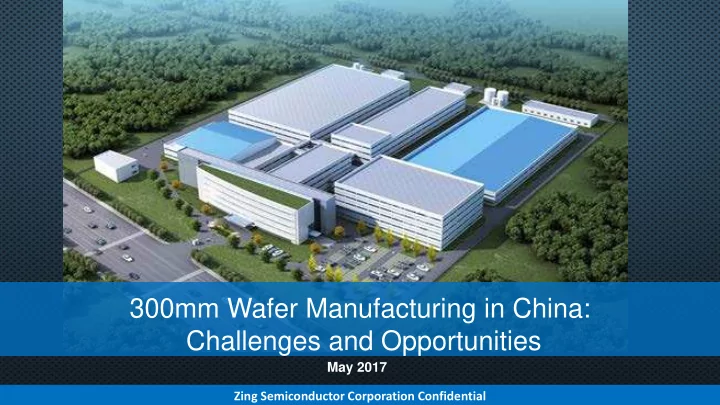
300mm Wafer Manufacturing in China: Challenges and Opportunities May 2017 Zing Semiconductor Corporation Confidential Agenda Advantages when working in China -Market -Policy Challenges when working in China - Partners - Localization A
300mm Wafer Manufacturing in China: Challenges and Opportunities May 2017 Zing Semiconductor Corporation Confidential
Agenda Advantages when working in China -Market -Policy Challenges when working in China - Partners - Localization A brief introduction to Zing Semiconductor Challenges for next-generation wafers Zing Semiconductor Corporation Confidential
Advantages when working in China -Market -Policy Challenges when working in China - Partners - Localization A brief introduction to Zing Semiconductor Challenges for next-generation wafers Zing Semiconductor Corporation Confidential
Semiconductor Market Forecast through 2020 14.9% 14.9% 8.0% 15.4% 15.0% 9.2% 15.3% 8.6% 9.2% 15.6% 9.4% 15.8% 9.2% 10.0% 15.3% 15.6% 15.7% 16.4% 9.8% 10.6% 10.0% 10.5% 10.7% 12.7% 15.0% 11.3% 13.7% 12.3% 11.3% 20.7% 14.5% 13.9% 14.2% 44.4% 56.2% 46.7% 41.4% 55.8% 57.5% 42.5% 51.9% 52.5% 54.7% 59.4% 12.1% 10.7% 10.0% 9.3% 9.4% 9.8% 9.2% 9.1% 9.6% 10.5% 12.6% SOURCE:IBS 4 Zing Semiconductor Corporation Confidential
China Semiconductor Consumption vs. Supply from Domestic Suppliers SOURCE:IBS Zing Semiconductor Corporation Confidential
2017 ~ 2020 New Fab Construction 62 new fabs have been announced as starting operation between 2017 and 2020. 26 of the new fabs are located in China, or 42% of the total. Zing Semiconductor Corporation Confidential
New Facility: Types By product type, the forecast for new facilities and lines include: ① 20 foundries (32 percent), ② 13 memory fabs (21 percent), ③ Seven LED (11 percent), ④ Six Power (10 percent) ⑤ Five MEMS (8 percent). Zing Semiconductor Corporation Confidential
Chinese 300mm wafer capacity, 2017-2020 2017 Current 300mm demand is from 8 manufacturers, with a combined 460kwpm production. Including test and monitor wafers, total wafer demand is between 500-550Kwpm . 2017-2020 Many fabs are scheduled to come online by 2020, including expansion of existing fabs as well as new players in the industry, including fabs in Hefei, Jinjiang, and Xiamen, among others. Demand for production wafers is expected to increase by 640K wpm, and including test and monitor wafers, demand is expected to increase by over 700K. By 2020 total wafer demand will be around 1.2M wpm. Red text above denotes fabs under construction Zing Semiconductor Corporation Confidential Zing Semiconductor Corporation Confidential 8
Advantages: Policy “Made in China 2025” Elements of Germany’s “Industry 4.0” policy Increased emphasis on supply chain efficiencies, supply chain communication, smart factories Collaboration with MNCs; move away from “indigenous innovation” for domestic market only Zing Semiconductor Corporation Confidential
Made in China 2025 - Financial / Facility support from central, provincial, and local governments - Focus on high-tech jobs creation, particularly in interior - Value-added raw materials highly desirable Zing Semiconductor Corporation Confidential
Advantages when working in China -Market -Policy Challenges when working in China - Partners - Localization A brief introduction to Zing Semiconductor Challenges for next-generation wafers Zing Semiconductor Corporation Confidential
Challenges: Finding the Right Partners - Picking the right location - Subcontractor quality - When and what to outsource Zing Semiconductor Corporation Confidential
Challenges: Localization - China GAAP vs. U.S. GAAP - Quality bilingual employees - Language of daily business? Zing Semiconductor Corporation Confidential
Advantages when working in China -Market -Policy Challenges when working in China - Partners - Localization A brief introduction to Zing Semiconductor Challenges for next-generation wafers Zing Semiconductor Corporation Confidential
Zing Semiconductor Zing Semiconductor is located in Lingang, a district of Shanghai, with a total area of 100,062 ㎡ . The total built-up area will be 128394.90 ㎡ . As of June 2018, investment will be $325M, with total investment estimated to be $1B at full capacity. Zing Semiconductor Corporation Confidential
2017-2022 Roadmap 2021-2022 Phase 3 2019-2020 Technology Node : 10nm and under Phase 2 Capacity: 600K Technology 300mm wafers per 2017-2018 Node : month 20nm~14nm Phase 1 Capacity : Technology Node : 300K 300mm 28nm wafers per Capacity : 150K month 300mm wafers per month Zing Semiconductor Corporation Confidential
To 150K wpm mass production 02: Const struction 03: R&D &D P Phase se 04: Ce Certif ificatio ion 05: Pha hase 1 e 1 End End * Production capacity of * Pass 4 to 5 * R&D equipment tender * Complete R & D 150k/month customers product * R&D equipment equipment installation * 6 months of sales of certification procurement * Complete product 100K wpm, monthly * Passed ISO9001 * Complete factory technology research and sales of 70 million RMB certification construction development * Complete 510 patent * Production capacity * Start customer sample 01: Planni nning ng applications of 80k/month manufacturing * Began wafer * Capacity to 10k wafers foundry services in per month *Complete Engineering January 2017 Design *Receive Production and Business Licenses 05 *Approval of construction 04 permits Phase 1 End 03 *Apply for 20 core patents 2017.10~2018.6 Certification 02 2017.1~2017.9 R&D Phase 01 2016.09~2016.12 Construction Planning 2015.10~2016.08 2014.06~2015.09 Zing Semiconductor Corporation Confidential
Crystal Growing Performance 2.0M Single Crystal 1.8M Single Crystal 1.6M Single Crystal Whole Single Crystal Whole Single Crystal Whole Single Crystal Pulling Speed 70mm 200mm ~ 1800mm: Target ± 4% 70mm ~ 1800mm: Target ± 8% Shoulder Shoulder Shoulder 100mm 100mm 100mm Ingot Axial Length [mm] Body Body 2000mm 1800mm Body 1600mm Tail Tail 300mm Tail 300mm 1800mm 300mm Date : 2016.12.28 Date : 2017.01.16 Date : 2017.02.13 Zing Semiconductor Corporation Confidential
Crystal Growing Performance Low COP Quality Summary 90nm LPDN Trend LPDN Result of Test-3 30 3000 2707.58 2500 20 2000 1500 12.6957 1000 10 500 313.889 2.26087 0.608696 0.521739 0.478261 2.26087 0 0 Test-1 Test-2 Test-3 37nm 65nm 90nm 120nm 200nm ☞ Production Date of Test-3 Ingot : 2017.4.01 37nm LPDN Result per Ingot Position 40 30 20 13.375 12.7 11.6 10 0 TOP MIDDLE BOTTOM Zing Semiconductor Corporation Confidential
Patent Applications Zing Semiconductor has applied for 304 patents, for crystal growth, silicon wafer substrate technology, epitaxial material growth, silicon III-V semiconductor material epitaxial growth, SOI wafer substrate preparation and advanced CMOS devices and processes, amongst others. It has received 36 patents, with the remaining patent applications still pending. Zing Semiconductor Corporation Confidential Zing Semiconductor Corporation Confidential 20
Quality Certification Plans 2015 2016 2017 Certification\ Time 11 12 1 2 3 4 5 6 7 8 9 10 11 12 1 2 3 4 5 6 7 8 9 10 11 12 ISO 9001:2015 ISO 14001:2004 2017/5 OHSAS 18001:2007 ISO/TS16949:2009 2017/9 Zing Semiconductor Corporation Confidential 23
Advantages when working in China -Market -Policy Challenges when working in China - Partners - Localization A brief introduction to Zing Semiconductor Challenges for next-generation wafers Zing Semiconductor Corporation Confidential
Challenges for the industry at 14nm and beyond - Growing demand for COP-free, starting with near-perfect crystal - Smaller edge exclusions Zing Semiconductor Corporation Confidential 23
Challenges for the industry at 14nm and beyond -Thick epi and FD-SOI SOURCE: Soitec SOURCE: Applied Materials Zing Semiconductor Corporation Confidential 23
Zing Semiconductor – Your source for 300mm wafers in China Richard Chang changrrg@zingsemi.com www.zingsemi.com 25 Zing Semiconductor Corporation Confidential
Recommend
More recommend
Explore More Topics
Stay informed with curated content and fresh updates.
