Testing and Boundary Scan Roth text: Chapter 10.1 10.4 Digital - PowerPoint PPT Presentation
Testing and Boundary Scan Roth text: Chapter 10.1 10.4 Digital circuit fault models Stuck-at fault: gate input/output appears to be always = logic 1 (stuck-at-1) or 0 (stuck at 0) Bridging fault: signal on one wire affects state
Testing and Boundary Scan Roth text: Chapter 10.1 – 10.4
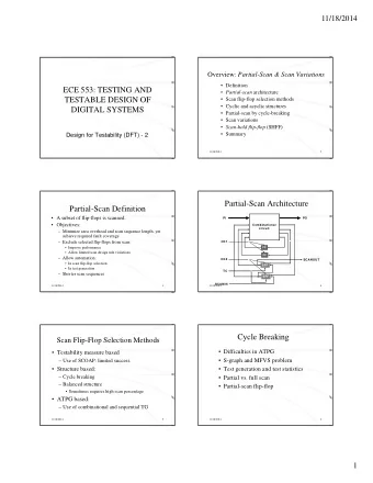
Digital circuit fault models • Stuck-at fault: gate input/output appears to be always = logic 1 (stuck-at-1) or 0 (stuck at 0) • Bridging fault: signal on one wire affects state of a second wire • Delay fault: logic states correct, but switching time longer than expected • Open circuit: open circuit on a wire • Short circuit
Testing for stuck-at faults “Test” – apply an input pattern (vector) that produces different values in fault-free and faulty circuits. a) Test a s-a-0 with vector 111 (expected output 1, erroneous output 0) b) Test a s-a-1 with vector 011 (expected output 0, erroneous output 1) c) Test a s-a-1 with vector 000 (expected output 0, erroneous output 1) d) Test a s-a-0 with vector 100 (expected output 1, erroneous output 0)
Test set to detect all stuck-at faults.
Sequential circuit testing From external inputs X(m), internal signals Q(n) difficult to control/set to desired value At external outputs Z(p), internal signals Q(n) difficult to observe/determine state
Scan path testing – improves controllability/observability During test (TCK clock): configure flip flops as a shift register (scan path) to load test patterns via input from SDI and observe flip flop states at output SDO. Normal operation (SCK clock): flip flop inputs/outputs connect from/to combinational ckt.
Circuit with and without scan chain One long scan path
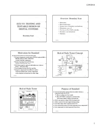
Boundary Scan (Text: Chap. 10.4) • Developed to test interconnect between chips on PCB – Originally referred to as JTAG (Joint Test Action Group) – Uses scan design approach to test external interconnect – No-contact probe overcomes problem of “in-circuit” test: • surface mount components with less than 100 mil pin spacing • double-sided component mounting • micro- and floating vias • Standardized test interface – IEEE standard 1149.1 Core – Four wire interface Application I/O buffer w/ BS cell • TMS - Test Mode Select Logic • TCK - Test Clock • TDI - Test Data In BS chain BS Int • TDO - Test Data Out • TRST - reset (optional & rarely included) TMS TCK TDI TDO
Use of boundary scan to detect shorts/opens between ICs Source: M. Smith Application-Specific IC’s, Figure 14.1
PC board test with boundary scan Link I/O cells of all ICs into one long scan chain
Boundary Scan Cell Architecture Basic BS Cell IN OUT MUX Bi-directional buffers S OUT MUX require multiple BS cells D Q D Q UPD CAP BS test data in (S IN ) CK CK S IN Shift_DR Capture_DR Update_DR Mode_Control Input data Input Cell to IC core BS Cell Operation Operational Data Control Tri-state control Cell From IC core Mode Transfer IN → OUT Normal Output data Output S IN → CAP Pad Scan From IC core Cell IN → CAP Capture CAP → UPD Update BS test data out (S OUT )
Boundary Scan Architecture Additional logic : • 1 Boundary Scan cell per I/O pin BS Chain (I/O buffers) • Test Access Port (TAP) MUX User Defined Registers – 4-wire interface TDI • MUX FF TDO TMS Bypass Register • TCK • TDI Instruction Decoder • TDO – TAP controller Instruction Register • 16-state FSM • controlled by TMS & TCK TMS – various registers for TAP TCK • Controller instructions • operations
Boundary Scan TAP Controller Operation Note: transitions 1 Test Logic Reset on rising edge 0 of TCK based 1 1 1 0 Run Test Idle Select DR Select IR on TMS value 0 0 1. Send test instruction serially Capture DR Capture IR 1 1 via TDI into Instruction 0 0 Register ( shift-IR ) 0 0 Shift DR Shift IR 1 1 2. Decode instruction and Exit-1 DR Exit-1 IR configure test circuitry 1 1 0 0 ( update-IR ) 0 0 Pause DR Pause IR 3. Send test data serially into 1 1 0 0 Exit-2 DR Exit-2 IR Data Register ( shift-DR ) via 1 1 TDI Update DR Update IR 4. Execute instruction ( update- 1 1 DR & capture-DR ) 0 0 5. Retrieve test results captured in Data Register ( shift-DR ) serially via TDO
Boundary Scan Instructions Defined by IEEE 1149.1 standard: • Mandatory Instructions – Extest – to test external interconnect between ICs – Bypass – to bypass BS chain in IC – Sample/Preload – BS chain samples external I/O; can shift patterns from TDI-BS-TDO while ckt operates – IDCode – 32-bit device ID • Optional Instructions – Intest – to test internal logic within the IC – RunBIST – to execute internal Built-In Self-Test • if applicable (this is rare) – UserCode – 32-bit programming data code • for programmable logic circuits – User Defined Instructions
Sample/Preload Instruction • Capture external inputs in BSR1/2 • Capture core outputs in BSR1/2
Extest instruction • Tests connections between IC pins • Previously: shift test pattern into BSR1/2 cells • Drive output pins with BSR2 (to external connections) and capture input pins in BSR1 (from external sources) • Later: shift out BSR1/2 to check for correct results
PCB interconnect test 1. Shift pattern into the 8 boundary scan cells via TDI - Test pattern bits in cells 3,4 of C1 and IC2 - Capture results in cells 1,2 of IC1 and IC2 2. Shift results out via TDO.
Intest instruction • Tests core logic • Previously: shift test patterns to BSR1/2 • Apply patterns to core logic inputs from BSR2 and capture core logic outputs in BSR1 • Later: shift out BSR1/2 to verify correct core outputs
Boundary Scan: User-Defined Instructions • User-defined instructions facilitate: – public instructions (available for customer use) – private instructions (for the manufacturer use only) – extending the standard to a universal interface • for any system operation feature or function • a communication protocol to access new IC test functions • In FPGAs – Access to configuration memory to program device – Access to FPGA core programmable logic & routing resources • Xilinx is one of few to offer this
Boundary Scan: Advantages • It’s a standard! (IEEE 1149.1) – allows mixing components from different vendors – provides excellent interface to internal circuitry • Supported by CAD tool vendors, IC & FPGA manufacturers • Allows testing of board & system interconnect – back-plane interconnect test w/o using PCB functionality – very high fault coverage for interconnect • Useful in diagnosis & FMA – provides component-level fault isolation – allows real-time sampling of devices on board – useful at wafer test (fewer probes needed) • BS path reconfigured to bypass ICs for faster access • IEEE P1500 uses BS circuitry around cores inside SoCs – TRST pin is not optional in order to initialize all cores
Boundary Scan: Disadvantages • Overhead: – Logic: about 300 gates/chip for TAP + about 15 gates/pin • overall overhead typically small (1-3%) • but significant for only testing external interconnect – especially tri-state (2 cells) & bi-directional buffers (3 cells) – I/O Pins: 4 • 5 if optional TRST (Test Reset) pin is included – Must be included in SoC cores to meet P1500 standards – I/O delay penalty • 1 MUX delay on all input & output pins – this can be reduced by design • Cannot test at system clock speed – But internal BIST can run at system clock speed
Labs 8/10 BScan Communications • As you serially shift in address and data on TDI via the USER2 port of the BSCAN module, the previous values you sent to the register file will shift out on TDO – As a sanity check, you can continue to shift in data and see it come out 6 clock cycles later in TDO in the Impact GUI • As you shift in the last bit of your address and data bring TMS high to Exit-DR and the next clock with TMS high will activate Update and load your data into the appropriate register in your register file – You can go back to Shift-DR to shift in a new set of address and data values for another register and repeat the process as long as you like without changing IR Note: the connections shown TDI TDI are for User Port #2 TDO TDO2 TCK DRCK2 Serial Data In Shift Shift Serial Data Out BSCAN Update Enable Parallel Data Out TMS SEL2 To LED Enable Signals are active only when Address & Data In instruction for user boundary To MUXs scan access is in IR C. E. Stroud ELEC 4200 Lab #8 22
Recommend
More recommend
Explore More Topics
Stay informed with curated content and fresh updates.

