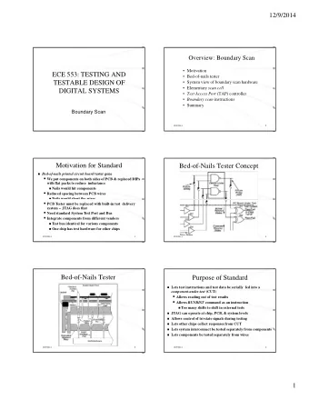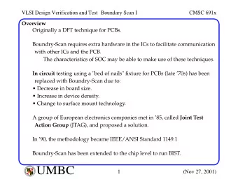
Boundary Scan Smith Text: Chapter 14.2 Top-down test design flow - PowerPoint PPT Presentation
Boundary Scan Smith Text: Chapter 14.2 Top-down test design flow BSDArchitect Source: FlexTest Manual Boundary-Scan Test JTAG (Joint Test Action Group) test standard became IEEE Standard 1149.1 Test Port and Boundary-Scan
Boundary Scan Smith Text: Chapter 14.2
Top-down test design flow BSDArchitect Source: FlexTest Manual
Boundary-Scan Test JTAG (Joint Test Action Group) test standard became IEEE Standard 1149.1 “Test Port and Boundary-Scan Architecture” Allows boards to be tested via 4 wires: TDI (test data input) TDO (test data output) TCK (test clock) TMS (test mode select) TRST (test reset) is optional Test data supplied serially via TDI & results checked via TDO, under control of TMS/TCK Some devices use boundary scan to: Download device configuration data (FPGAs) Download program code (microcontrollers) Interface to on-chip BIST and debug circuits
Use of boundary scan to detect shorts/opens between ICs Smith text figure 14.1
JTAG/IEEE 1149.1 Boundary Scan Basic Structure Source: Mentor Graphics “Boundary Scan Process Guide”
Chip-level boundary scan architecture Source: Mentor Graphics “Boundary Scan Process Guide”
Data register (boundary) cell data flow Normal mode (mode= 0) : data_in to data_out * Chip input pin: data_in from board, data_out to chip * Chip output pin: data_in from chip, data_out to board Also used in “Bypass” mode
Data register (boundary) cell data flow Scan mode: scan_in to capture FF , capture FF to scan_out shiftDR= 1 & clockDR pulse TDI drives first scan_in signal in chain Last scan_out in chain drives TDO
Data register (boundary) cell data from board/ chip Capture mode: data_in captured in “capture FF” shiftDR= 0 & clockDR pulse data_in from board (extest) – chip input pin data_in from chip (intest) – chip output pin
Data register (boundary) cell “Update Mode”: data from capture FF to update FF updateDR= 1 Save scan chain values in update FFs to apply to data_out later during EXTEST/INTEST
Data register (boundary) cell data to board/ chip Drive mode: update FF to data_out mode= 1 data_out to board (extest) – chip output pin data_out to chip (intest) – chip input pin
Boundary-scan instructions EXTEST external test of chip-chip connections SAMPLE/PRELOAD sample values from input pads during capture preload BSC update register during update BYPASS scan data through 1-cell bypass register other BSC’s pass data_in to data_out Load/decode in Instruction Register
TAP controller state diagram TDI -> DR TDI -> IR State changes controlled by TMS & TCK Smith Text: Figure 14.7
Boundary-scan example Smith Text: Figure 14.9
Boundary-scan tools Mentor Graphics/Tessent “BSDArchitect” synthesize boundary-scan circuits insert boundary-scan circuits generate boundary-scan test vectors generate Verilog test bench BSDL Boundary-Scan Description Language Subset of VHDL - describes features of IEEE 1149.1 Use in test generation software
External Mode Wrap BSD circuit around your design
Internal Mode • Add boundary scan internal to your design • Place TAP controller and BSD cells within top level
BSDAdvisor “external” design flow
Recommend
More recommend
Explore More Topics
Stay informed with curated content and fresh updates.

