Ten Years of the CDF Silicon Vertex Detector: Ten Years of the CDF - PowerPoint PPT Presentation
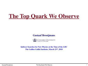
Ten Years of the CDF Silicon Vertex Detector: Ten Years of the CDF Silicon Vertex Detector: Performance and Status Performance and Status Miguel N. Mondragon Fermilab On behalf of the CDF Silicon Group May 31, 2011 New Perspectives 2011
Ten Years of the CDF Silicon Vertex Detector: Ten Years of the CDF Silicon Vertex Detector: Performance and Status Performance and Status Miguel N. Mondragon Fermilab On behalf of the CDF Silicon Group May 31, 2011 New Perspectives 2011 Fermilab
Overview Overview Overview of the Silicon Detectors at CDF Radiation Damage Global Performance Conclusions 1 “The CDF Silicon Detector: Performance and Status” – MN Mondragon – New Perspectives 2011.
Tevatron and CDF Tevatron and CDF Tevatron Scheduled end of operations: September, 2011 Present delivered luminosity: ~11 fb -1 Expected delivered luminosity at the end of operations: ~12 fb -1 CDF Much of the physics program depends on Heavy-Flavor tagging (top- , b-quark physics, low-mass Higgs boson search) Silicon detectors essential for vertex positioning of HF decays 2 “The CDF Silicon Detector: Performance and Status” – MN Mondragon – New Perspectives 2011.
The Silicon Detector The Silicon Detector Three microstrip subdetectors, “p” strips on “n” bulk ISL: longer in z for forward coverage SVX II: the main subdetector (~60% of } } the channels) Beam line L00: mounted on the beam pipe 7-8 concentric layers 7 m 2 of silicon 722,432 channels 3 “The CDF Silicon Detector: Performance and Status” – MN Mondragon – New Perspectives 2011.
The L00 Subdetector The L00 Subdetector cables SVX innermost SVX inner bore layer Silicon sensors Beam pipe 1.1 cm Cooling tube channel C fiber support Mounted directly on the beam pipe Designed to improve track impact parameter resolution Single sided sensors (axial strips). Readout strip pitch 50 μ m Modules by three manufacturers: Hamamatsu , 36 “wide” modules at r=1.62 cm SGS Thomson, 10 “narrow” modules at r=1.35 cm Micron, 2 “narrow” modules (oxygenated – more radiation tolerant) 4 “The CDF Silicon Detector: Performance and Status” – MN Mondragon – New Perspectives 2011.
The SVX II Subdetector The SVX II Subdetector Double sided sensors (built-in strips on both sides) for φ and z positioning Radial segmentation: 5 layers φ segmentation: 12 wedges Axial segmentation: 6 bulkheads wedge Strip pitch 60-140 µ m Radius: 2.5 to 10.7 cm SVX-Layer 0 (72 sensors) Hamamatsu, Layers 0, 1, 3. Axial ( φ )/z strips Micron, Layers 2, 4. Axial/small-angle stereo strips “The CDF Silicon Detector: Performance and Status” – MN Mondragon – New Perspectives 2011. 5
The ISL Subdetector The ISL Subdetector 1 m Located between SVX II and the central drift chamber (COT) Designed to improve track reconstruction and linking to the central drift chamber (especially at forward coverage ) Three layers central (| η| < 1) and r = 22 cm Forward (1 < | η| < 2) and r = 20 cm Forward (1 < | η| < 2) and r = 28 cm Double sided sensors (axial and small-angle stereo strips) 6 “The CDF Silicon Detector: Performance and Status” – MN Mondragon – New Perspectives 2011.
Basic Principle of Silicon Strip Sensors Basic Principle of Silicon Strip Sensors Single sided sensor -V dep Integration, amplification, digitization,... (SVX3D chip) Electrical signal Metal strips Insulator (SiO 2 ) Implant strips (p + -doped) + – + E-field μ – 300 m Bulk (n-doped) + – + – Backplane (n + -doped) Charged particle Reversed bias voltage Full depletion gives the maximum collection of charges (minimizes recombination) 7 “The CDF Silicon Detector: Performance and Status” – MN Mondragon – New Perspectives 2011.
Radiation Damage Radiation Damage
Tracking Volume Radiation Field Tracking Volume Radiation Field The radiation field has been measured and modeled at CDF using 916 dosimeters (TLDs), R.J. Tesarek et al. , NIM A514, 188 (2003) Locations of 916 Thermal Luminescent Dosimeters ( TLDs) in the CDF tracking volume. 8 “The CDF Silicon Detector: Performance and Status” – MN Mondragon – New Perspectives 2011.
A Model of Radiation Damage A Model of Radiation Damage In addition to ionization, part of the radiation produces crystal defects Some complex crystal defects with vacancies can trap electrons and change the electrical properties by removing donors and creating acceptors ∆ N eff ( Φ , t,T ) = ∆ N C ( Φ ) + ∆ N Y ( Φ , t,T ) Parametrization: ∆ N Y ( Φ , t,T ) = g Y Φ [ 1−1/(1+t/ τ Y (T)) ] ∆ N C ( Φ ) = N C0 (1−e −c Φ )+g C Φ, With sufficient radiation the “n” bulk M.Moll (1992) turns into a “p-like” bulk Data from test beam Type inversion Depletion voltage follows the concentration of “dopants” Depletion V dep ~ |N eff | d 2 Voltage M.Moll, PhD Thesis , (1992) Uni Hamburg; Fluence Φ eq [10 12 cm -2 ] papers by RD2, RD50 Collaborations,... 9 “The CDF Silicon Detector: Performance and Status” – MN Mondragon – New Perspectives 2011.
Radiation Damage on Operations Radiation Damage on Operations Observable effects of Radiation Damage Increased depletion voltage (above a minimum) Lower Signal-to-Noise ratio (smaller collected Signal, larger Noise) Increased reversed-bias current Operational Implications Increased bias voltage required Limitations on voltage: power supply limit, sensor breakdown Signal-to-Noise ratio must be kept good enough for physics analyses The CDF Silicon Detector was designed to withstand radiation up to ~ 3 fb -1 of integrated luminosity 10 “The CDF Silicon Detector: Performance and Status” – MN Mondragon – New Perspectives 2011.
Evolution of Depletion Voltage Evolution of Depletion Voltage Linear rise Inversion As radiation damage increases: Point (minimum) Required depletion voltage rises Need to increase reversed-bias V to keep good efficiency Measured V dep at different integrated luminosities: Fit a 3 rd degree polynomial around minimum Linear fit above inversion point The linear rise can be extrapolated to make predictions... 11 “The CDF Silicon Detector: Performance and Status” – MN Mondragon – New Perspectives 2011.
Outlook of Depletion Voltage for L00 Outlook of Depletion Voltage for L00 Linear fits and extrapolations for ALL sensor modules of L00: Operational limit at ~500 V A few sensors are reaching the operational limit for a full V dep and becoming under-depleted 12 “The CDF Silicon Detector: Performance and Status” – MN Mondragon – New Perspectives 2011.
Conversion of Luminosity to Radiation Dose for L00 Conversion of Luminosity to Radiation Dose for L00 CDF Preliminary Average V dep (over all sensors) [V] Hamamatsu (wide) SGS Thomson (narrow) Micron oxygenated (narrow ) Using the measured radiation field and knowing the position of the silicon sensors, it is possible to convert luminosity to radiation dose The (oxygenated) Micron sensors inverted after the others, as expected 13 “The CDF Silicon Detector: Performance and Status” – MN Mondragon – New Perspectives 2011.
Depletion Voltage for SVX - L0 Depletion Voltage for SVX - L0 CDF Preliminary Average V dep (over all sensors) [V] SVX-L0 Operational limit: sensors may break down at V bias > 170 V Some ladders may become under-depleted soon 14 “The CDF Silicon Detector: Performance and Status” – MN Mondragon – New Perspectives 2011.
Global Performance Global Performance
Signal-to-Noise ratios for L00 and SVX Signal-to-Noise ratios for L00 and SVX Signal measured from data events J/ Ψ to muons Noise estimated from calibration runs with beam φ side z side b -tagging b -tagging requirement (S/N > 4) 11 12 11 12 Now S/N will be still good for b-tagging End of SVX-L0 degrades the fastest collisions 15 “The CDF Silicon Detector: Performance and Status” – MN Mondragon – New Perspectives 2011.
How much does a dead SVX-L0 impact b-tagging? How much does a dead SVX-L0 impact b-tagging? b-tagging efficiency Bulkhead 0 Bulkhead 3 Bulkhead 1 Average (excluding Bulkhead 4 encircled wedges) Bulkhead 2 Bulkhead 5 Wedge Number Wedge Number Plot depicts b-tagging efficiencies estimated with data, for jets whose axis passes through SVX -L0 Blue circles indicate wedge where sensor in layer L0 is not taking data Green circles indicate whole wedge (all layers) is not taking data The dead of a layer L0 sensor would not degrade the efficiency so much! 16 “The CDF Silicon Detector: Performance and Status” – MN Mondragon – New Perspectives 2011.
Active Modules 2002-2011 Active Modules 2002-2011 The silicon system is getting good data from ~86% of the sensors and running b -1 b -1 ~92.5% of the detector. f f 3 7 Powered in black, good in green , bad in red and error rate in pink 17 “The CDF Silicon Detector: Performance and Status” – MN Mondragon – New Perspectives 2011.
Conclusions Conclusions The CDF Silicon Detectors have outlasted their expected lifespan... and are still in good shape! Some sensors may become under-depleted soon in L00 and SVX-L0, but will continue in operation S/N ratio will still be good for b-tagging until the end of online operations Tomorrow in the Poster Session: Aging Kyle Knoepfel, studies “Aging Studies of the CDF Run II Silicon Detector” Operational Tim Harrington-Taber, experience “Operational Experience of the CDF Run II Silicon Detector” 18 “The CDF Silicon Detector: Performance and Status” – MN Mondragon – New Perspectives 2011.
Back-up Slides Back-up Slides
Recommend
More recommend
Explore More Topics
Stay informed with curated content and fresh updates.
