Quantum Capacitance Quantum Capacitance in Scaled-Down III-V FETs - PowerPoint PPT Presentation
Quantum Capacitance Quantum Capacitance in Scaled-Down III-V FETs Donghyun Jin, Daehyun Kim * , Taewoo Kim and g y , y , Jess A. del Alamo Microsystems Technology Laboratories y gy Massachusetts Institute of Technology * Presently with
Quantum Capacitance Quantum Capacitance in Scaled-Down III-V FETs Donghyun Jin, Daehyun Kim * , Taewoo Kim and g y , y , Jesús A. del Alamo Microsystems Technology Laboratories y gy Massachusetts Institute of Technology * Presently with Teledyne Scientific Acknowledgement: FCRP-MSD Center, Intel 1
Overview Overview 1 Motivation 1. Motivation 2. Gate Capacitance Model for III-V FETs 3 M 3. Measurements of C G on InGaAs HEMTs t f C I G A HEMT 4. Comparison of Model and Experiments 5. Projection for 10 nm III-V MOSFETs 6 Conclusions 6. Conclusions 2
1 Motivation : III-V CMOS 1. Motivation : III V CMOS III-V MOSFET Gate III ‐ V Channel Source Drain • III-V CMOS: III-V semiconductor in channel - High electron velocity � Low effective mass (m * ) 3
1 Motivation : III-V CMOS 1. Motivation : III V CMOS III-V MOSFET Gate III ‐ V Channel Source Drain • III-V CMOS: III-V semiconductor in channel - High electron velocity � Low effective mass (m * ) • Low m * � small Density of States (DOS) Low m � small Density of States (DOS) � low sheet carrier concentration (N S ) in channel • Will III-V CMOS attain required N S Will III V CMOS attain required N at the 10 nm node? 4
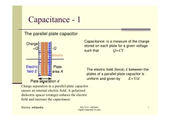
Gate Capacitance Gate Capacitance in III-V MOSFET C cent III-V MOS III V MOS V V G V G C Gate E C C ins ψ ψ ins ψ S S Insulator E F S C C Q C Q III ‐ V Channel inv C Metal III-V Channel cent Insulator • Inversion-layer capacitance (C inv ) is series of - Quantum capacitance (C Q ): Quantum capacitance (C ): � E F penetration in CB, proportional to DOS - Centroid capacitance (C cent ): � Finite distance of electrons away from interface � Finite distance of electrons away from interface 5
Gate Capacitance Gate Capacitance in III-V MOSFET C cent III-V MOS III V MOS V V G V G C Gate E C C ins ψ ψ ins ψ S S Insulator E F S C C Q C Q III ‐ V Channel inv C Metal III-V Channel cent Insulator • Inversion-layer capacitance (C inv ) is series of - Quantum capacitance (C Q ): Quantum capacitance (C ): � E F penetration in CB, proportional to DOS - Centroid capacitance (C cent ): � Finite distance of electrons away from interface � Finite distance of electrons away from interface m* ↓ � DOS ↓ � C Q ↓ � Problem in III-V MOSFET? 6
Gate Capacitance in III-V HEMTs Gate Capacitance in III V HEMTs Goal: Experimental and theoretical study of C G in III-V HEMTs III-V High Electron Mobility Transistor L L G Source Drain Barrier Si δ doping t ins Channel t ch t ins = Barrier thickness t ch = Channel thickness Buffer • Experimentally extract C G for HEMTs with different t ins and t ch • Build C G model including DOS effect • Project C G and N S of scaled down III-V FETs 7
Experimental HEMT Cross Section Experimental HEMT Cross Section Metal PR PR Gate Gate Barrier = In 0.52 Al 0.48 As (4 or 10 nm) S D Oxide Channel = In 0.53 Ga 0.47 As (2 nm) Cap Channel = In 0.7 Ga 0.3 As (8 nm) Channel= In Ga As (8 nm) Etch stopper Etch stopper Core or InAs (5 nm) Barrier t ins t ch Channel Channel = In 0.53 Ga 0.47 As (3 nm) t ch = 10 nm Buffer Buffer = In 0.52 Al 0.48 As (~400 nm) L L G = 30 nm 30 Substrate = InP (~300 nm) Type B HEMT • Three different heterostructures explored : t ins (nm) t ch (nm) Channel Core Reference L G range (nm) Type A 10 10 InAs (5 nm) Kim, unpublished 40 ~ 100 Type B 4 10 0 InAs (5 nm) ( ) Kim, IEDM 2008 i 2008 30 30 ~ 200 200 Type C 4 13 In 0.7 Ga 0.3 As (8 nm) Kim, IEDM 2006 40 ~ 100 8
2. Gate Capacitance Model p C C ins ψ ins ψ S S C C ins ψ C C S … … 1 Q 2 Q C C C inv 1 2 inv inv C C 2 cent cent cent 1 1 1 st Subband 2 nd Subband 1 st Subband 2 nd Subband ∂ − ( ( ) ) 1 Q Q ∑ ∑ = = S S C C ∂ ψ inv 1 1 + i S C C _ _ Q i cent i 9
2. Gate Capacitance Model p C C ins ψ ins ψ S S C C ins ψ C C S … … 1 Q 2 Q C C C inv 1 2 inv inv C C 2 cent cent cent 1 1 1 st Subband 2 nd Subband 1 st Subband 2 nd Subband ∂ − ( ( ) ) 1 Q Q ∑ ∑ = = S S C C ∂ ψ inv 1 1 + i S C C _ _ Q i cent i Quantum capacitance 2D DOS Centroid capacitance * 2 m q of subband i of subband i || ∂ − π π � ( ) E E 2 = = = ⋅ ∂ F i C C C C C C − − _ _ _ cent i Q i Q i E E ( ) E E + 1 exp( i F ) i C kT 10
Verification of Physical Model Verification of Physical Model Type A • Solid line : 12 I G A InGaAs (t ch = 13 nm, t ins = 4nm) (t 13 t 4 ) Numerical simulation results 10 Type B from 1D Poisson-Schrodinger InAs (t ch = 10 nm, t ins = 4 nm) solver (Nextnano) 8 m 2 ] C G [fF/ μ m Type C (- ) d Q 6 = InAs S C (t ch = 10 nm, t ins = 10 nm) G dV 4 G • Symbols : 2 Physical model results 0 (using Nextnano to extract E i ) (using Nextnano to extract E i ) -0.4 0 4 -0.2 0 2 0 0 0.2 0 2 0 4 0.4 V G [V] Good agreement g between model and numerical simulations 11
3. Experimental C G in a HEMT obtained from S – parameter measurements f S Type B Gate Small V DS 3000 V GS = 0.4 V V DS = 10 mV ½ C gext [fF/mm] ½ C gext 0.35 2500 L G 0 3 0.3 G (V GS = -0.3 V) 2000 C gi Barrier 1500 0.25 Channel 1000 C G - C G 0.2 Parasitic Gate Capacitance Intrinsic Gate Capacitance 500 Slope = C gi 0 C G (in fF/ μ m) = C gi (in fF/ μ m 2 ) x L G + C gext 0 50 100 150 200 250 L G [nm] L [nm] C gi = Slope of C G - C G (V G = -0.3V) with L G G ( ) gi G G G 12
Experimental Intrinsic Gate Capacitance Experimental Intrinsic Gate Capacitance 15 Type B Type B 10 μ m 2 ] Type C C gi [fF/ μ 5 Type A 0 -0.3 -0.2 -0.1 0 0.1 0.2 0.3 V V G [V] [V] Comparison with physical model: y C ins , C Q , C cent contribution to C gi 13
4. Comparison of measurements and model : T Type A (InAs channel, t ch = 10 nm, t ins = 10 nm) A (I A h l t 10 t 10 ) 50 0 8 0.8 Experiment (C G ) 40 0.6 F/ μ m 2 ] E 2 C cent1 V] E i - E F [eV 30 30 0 4 0.4 apacitance [fF C Q1 E 1 0.2 20 C inv1 C ins (t ins = 10 nm) E F E F Ca 0 10 C G C inv2 -0.2 0 -0.4 -0.2 0 0.2 0.4 -0.4 -0.2 0 0.2 0.4 V V G [V] [V] V G [V] • Good agreement between measurements and model • C ins comparable to C inv � C G ~ 62% of C ins C bl t C � C 62% f C • Only 1 st subband populated 14
Comparison of measurements and model : Type B (InAs channel, t ch = 10 nm, t ins = 4 nm) T B (I A h l t 10 t 4 ) 50 0.8 Experiment (C ) Experiment (C G ) 40 0.6 [fF/ μ m 2 ] E 2 C ins (t ins = 4 nm) [eV] 30 0.4 Capacitance E i - E F [ E 1 20 0.2 C Q1 C inv1 C cent1 E F 0 0 10 10 C G C inv2 -0.2 0 -0.4 -0.2 0 0.2 0.4 -0.4 -0.2 0 0.2 0.4 V G [V] V G [V] G • Moderate agreement • C Q1 < C ins � C G limited by C Q1 : C G ~ 47% of C ins y Q1 ins G Q1 G ins • Only 1 st subband populated 15
Comparison of measurements and model : Type C (In 0.7 Ga 0.3 As channel, t ch = 13 nm, t ins = 4 nm) T C (I G A h l t 13 t 4 ) 50 0.8 Experiment (C ) Experiment (C G ) 40 0.6 [fF/ μ m 2 ] E 2 C ins (t ins = 4 nm) [eV] 30 0.4 E i - E F [ Capacitance C Q1 E 1 20 0.2 C inv1 C cent1 E F C G 10 0 0 C inv2 0 -0.2 -0.4 -0.2 0 0.2 0.4 -0.4 -0.2 0 0.2 0.4 V G [V] V G [V] G • Good agreement • Thicker channel: C cent1 comparable to C ins � C G ~ 35% of C ins • 1 st subband dominant, 2 nd subband minor 16
Summary of Key Findings Type A Type B Type C (InAs , t ch = 10 nm, t ins = 10 nm) (InAs , t ch = 10 nm, t ins = 4 nm) (In 0.7 Ga 0.3 As, t ch = 13 nm, t ins = 4 nm) 50 50 50 Experiment (C G ) Experiment (C G ) Experiment (C G ) 40 40 40 itance [fF/ μ m 2 ] itance [fF/ μ m 2 ] tance [fF/ μ m 2 ] C cent1 C ins ( t ins = 4 nm) C ins ( t ins = 4 nm) 30 30 30 C Q1 C Q1 20 20 20 20 20 20 C C Q1 Capaci Capaci Capac C inv1 C inv1 C inv1 C cent1 C ins ( t ins = 10 nm) C cent1 C G 10 10 10 C G C G C inv2 C inv2 C inv2 0 0 0 -0.4 -0.2 0 0.2 0.4 -0.4 -0.2 0 0.2 0.4 -0.4 -0.2 0 0.2 0.4 V V G [V] [V] V G [V] V G [V] • Finite C inv severely reduces C G below C ins • C Q1 smallest in lower m* channel Q1 • 1 st subband dominates • C cent1 relevant: t ch ↓ � C cent1 ↑ 17
Summary of Key Findings Type A Type B Type C (InAs , t ch = 10 nm, t ins = 10 nm) (InAs , t ch = 10 nm, t ins = 4 nm) (In 0.7 Ga 0.3 As, t ch = 13 nm, t ins = 4 nm) 50 50 50 Experiment (C G ) Experiment (C G ) Experiment (C G ) 40 40 40 itance [fF/ μ m 2 ] itance [fF/ μ m 2 ] tance [fF/ μ m 2 ] C cent1 C ins ( t ins = 4 nm) C ins ( t ins = 4 nm) 30 30 30 C Q1 C Q1 20 20 20 20 20 20 C Q1 C Capaci Capaci Capac C inv1 C inv1 C inv1 C cent1 C ins ( t ins = 10 nm) C cent1 C G 10 10 10 C G C G C inv2 C inv2 C inv2 0 0 0 -0.4 -0.2 0 0.2 0.4 -0.4 -0.2 0 0.2 0.4 -0.4 -0.2 0 0.2 0.4 V V G [V] [V] V G [V] V G [V] • Finite C inv severely reduces C G below C ins • C Q1 smallest in lower m* channel Q1 • 1 st subband dominates • C cent1 relevant: t ch ↓ � C cent1 ↑ C ( C G (exp) > C G (model) in Type B, Why? ) C ( d l) i T B Wh ? � C Q1 most relevant in Type B 18
Source of Discrepancy for C G in Type B p y yp G 1.Uncertainty in t ins - ±0.5 nm error margin from TEM g 2. Increase of in-plane effective mass (m || * ) - Biaxial channel strain + Non-parabolicity + Quantization [Theory : Nag APL 1993; Experiment : Wiesner APL 1994] [Theory : Nag APL 1993; Experiment : Wiesner APL 1994] 19
Recommend
More recommend
Explore More Topics
Stay informed with curated content and fresh updates.
