Crosstalk - How can we avoid it - Herv Grabas Mutual Inductance and - PowerPoint PPT Presentation
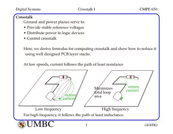
Crosstalk - How can we avoid it - Herv Grabas Mutual Inductance and Capacitance Crosstalk is the coupling of energy from one line to another via: Mutual capacitance (electric field) Mutual inductance (magnetic field) Mutual Inductance, L
Crosstalk - How can we avoid it - Hervé Grabas
Mutual Inductance and Capacitance Crosstalk is the coupling of energy from one line to another via: Mutual capacitance (electric field) Mutual inductance (magnetic field) Mutual Inductance, L m Mutual Capacitance, C m Zo Zo Zo Zo far far C m L m near Zs near Zs Zo Zo
Mutual Inductance and Capacitance “ Mechanism of coupling” The circuit element that represents this transfer of energy are the following familiar equations dI dV Lm Cm V L I C m m dt dt The mutual inductance will induce current on the victim line opposite of the driving current (Lenz’s Law) The mutual capacitance will pass current through the mutual capacitance that flows in both directions on the victim line Crosstalk Overview
Crosstalk Induced Noise “ Coupled Currents” The near and far end victim line currents sum to produce the near and the far end crosstalk noise Zo Zo Zo Zo far far I Cm I Lm L m near Zs near Zs Zo Zo I I I I I I near Cm Lm far Cm Lm
Crosstalk Induced Noise “ Voltage Profile of Coupled Noise” Near end crosstalk is always positive Currents from Lm and Cm always add and flow into the node For PCB’s, the far end crosstalk is “usually” negative Current due to Lm larger than current due to Cm Note that far and crosstalk can be positive Zo Zo Far End Driven Line Un-driven Line “victim” Zs Near End Driver Zo
Graphical Explanation Time = 0 Near end crosstalk pulse at T=0 (I near ) ~Tr Near end V crosstalk Zo TD Far end crosstalk pulse at T=0 (I far ) ~Tr Time= 1/2 TD 2TD V Zo far end crosstalk Zo Time= TD V Far end of current Zo Zo terminated at T=TD Time = 2TD V Near end current Zo terminated at T=2TD Zo Crosstalk Overview
Crosstalk Equations TD Zo V L C input M M A Terminated Victim Zo 4 L C TD Far End X LC Driven Line V X LC L C Un-driven Line input M M B “victim” 2 T L C A r B Zs Near End Driver Zo Tr ~Tr Tr TD 2TD Far End Zo Open Victim V L C input M M A Far End 4 L C Driven Line Un-driven Line 1 “victim” A B C B 2 C Zs Near End Driver V X LC Zo ~Tr ~Tr L C Tr input M M C T L C r 2TD Crosstalk Overview
Creating a Crosstalk Model “ Equivalent Circuit” The circuit must be distributed into N segments C 12 L Line 2 Line 1 K 12 L L C 1G C 2G 11 22 L11(2) L 11 (N) L 11 (1) Line 1 C 1G (1) C 1G (2) C 1G (N) K1 K1 K1 C 12 (2) C 12 (n) C 12 (1) Line 2 L 22 (2) L 22 (N) L 22 (1) C 2G (1) C 2G (N) C 2G (2) Crosstalk Overview
Odd and Even Transmission Modes Electromagnetic Fields between two driven coupled lines will interact with each other These interactions will effect the impedance and delay of the transmission line A 2-conductor system will have 2 propagation modes Even Mode (Both lines driven in phase) Odd Mode (Lines driven 180 o out of phase) Even Mode Odd Mode The interaction of the fields will cause the system electrical characteristics to be directly dependent on patterns Crosstalk Overview
Odd Mode Transmission Potential difference between the conductors lead to an increase of the effective Capacitance equal to the mutual capacitance +1 -1 +1 -1 Electric Field: Magnetic Field: Odd mode Odd mode Because currents are flowing in opposite directions, the total inductance is reduced by the mutual inductance (Lm) dI d ( I ) V Drive (I) V L Lm dt dt dI I Induced (-I Lm ) Lm ( L Lm ) Induced (I Lm ) dt Drive (-I) -I
Even Mode Transmission Since the conductors are always at a equal potential, the effective capacitance is reduced by the mutual capacitance +1 +1 +1 +1 Magnetic Field: Electric Field: Even mode Even mode Because currents are flowing in the same direction, the total inductance is increased by the mutual inductance (Lm) dI d ( I ) V Drive (I) V L Lm dt dt dI I Induced (I Lm ) ( L Lm ) Lm Induced (I Lm ) dt Drive (I) I
Termination Techniques Pi and T networks Single resistor terminations described in chapter 2 do not work for coupled lines 3 resistor networks can be designed to terminate both odd and even modes T Termination +1 R 1 Odd Mode Equivalent -1 R 1 R 2 R 3 R 2 Virtual Ground in center -1 2R 3 +1 R R Z Even Mode R 1 1 2 odd Equivalent 1 +1 2 R Z Z 2R 3 3 even odd R 2
Termination Techniques Pi and T networks The alternative is a PI termination PI Termination R 1 R 1 +1 ½ R 3 Odd Mode R 3 Equivalent -1 ½ R 3 R 2 R 2 -1 +1 R 1 Even Mode R R Z 1 2 even Equivalent +1 R 2 Z Z 2 even odd R 3 Z Z even odd
Formula : near end cross talk Near end cross talk is usually dominant
Formula far end cross talk
Odd and even impedance Impedance Variation for a Three Conductor Stripline (Width=5[mils]) 120 Impedance[Ohms] 100 80 60 40 20 0 5 10 15 20 Edge to Edge Spacing [mils] Z single bit states Z even states Z odd states
Some results
Some results 4GHz of bandwidth -10dB of coupling up to Jason & Ossy ceramic plate 2.3GHz
Some results
Some results 800MHz of bandwidth -10dB of coupling up to LAPPD glass plate 300MHz
Conclusion More work needed on the coupling. Plan : • Look back at the odd and even mode impedance values • Make a Pi termination • Create a model of the coupling and test it
Different topic: MCP simulation Can we create a model of this?
The answer is yes This is for a perfect Dirac distributed current with constant velocity
Plot of previous function 3dB = 1.14GHz Parameters : High voltage across gap V = 100V Gap = 1e-3 m
This is for a perfect Dirac distributed current with constant acceleration
Plot of previous function 3dB = 2.3GHz
Case of space distributed charge This is for a Rect distributed over a distance s current with constant speed
3dB = 830MHz Space charge : the small the electron cloud spreading the better
Recommend
More recommend
Explore More Topics
Stay informed with curated content and fresh updates.


![Speaker 1: Good afternoon. Can everybody hear me? [crosstalk 00:00:12] Hello everyone. We're going](https://c.sambuz.com/107234/speaker-1-good-afternoon-can-everybody-hear-me-crosstalk-s.webp)
