PVMD Arno Smets Delft University of Technology Learning objectives - PowerPoint PPT Presentation
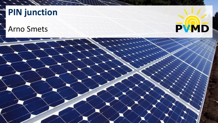
PIN junction PVMD Arno Smets Delft University of Technology Learning objectives What is a PIN junction Why is a PIN junction used for thin film silicon solar cells Importance of doped layers Charge carrier transport mechanisms
PIN junction PVMD Arno Smets Delft University of Technology
Learning objectives • What is a PIN junction • Why is a PIN junction used for thin film silicon solar cells • Importance of doped layers
Charge carrier transport mechanisms Drift Diffusion Charge carrier density _ P-type _ E-Field + N-type + position
Diffusion length c-Si a-Si:H L D ~ 300 μ m L D < 300 nm
Charge carrier transport mechanisms Drift Diffusion Charge carrier density _ P-type _ E-Field + N-type + position
PIN junction Intrinsic a-Si:H n-a-Si:H p-a-SiC:H Conduction band E Fermi Valence band
PIN junction Intrinsic a-Si:H n-a-Si:H p-a-SiC:H _ E Fermi +
PIN cell Glass superstrate p TCO + _ i p-a-SiC:H i-a-Si:H n-a-Si:H n Metal back contact
PIN cell Doped layer requirements : p 1. Optimal refractive index + _ i 2. High bandgap energy 3. Adequate transverse n conductivity
Drift Diffusion Window layer requirements : Charge carrier density 1. Optimal refractive index _ P-type 2. High bandgap energy _ E-Field + N-type 3. Adequate transverse conductivity + position glass p TCO p-a-SiC:H + _ i i-a-Si:H n-a-Si:H ZnO/SiO x back reflector Metal back contact n
Recommend
More recommend
Explore More Topics
Stay informed with curated content and fresh updates.

