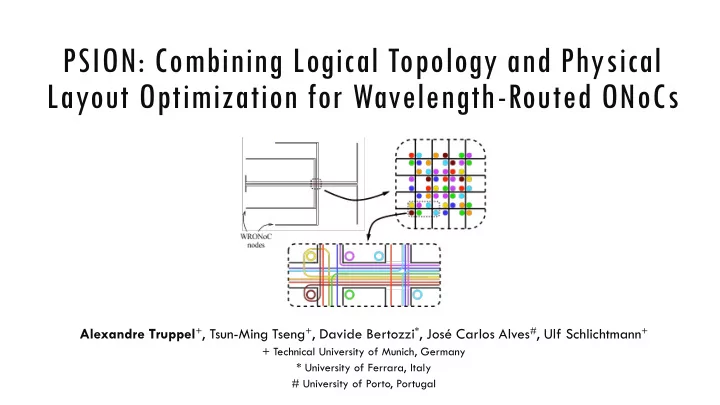
PSION: Combining Logical Topology and Physical Layout Optimization - - PowerPoint PPT Presentation

psion combining logical topology and physical layout
SMART_READER_LITE
LIVE PREVIEW

PSION: Combining Logical Topology and Physical Layout Optimization - - PowerPoint PPT Presentation

PSION: Combining Logical Topology and Physical Layout Optimization for Wavelength-Routed ONoCs Alexandre Truppel + , Tsun-Ming Tseng + , Davide Bertozzi * , Jos Carlos Alves # , Ulf Schlichtmann + + Technical University of Munich, Germany *


slide-1
SLIDE 1

PSION: Combining Logical Topology and Physical Layout Optimization for Wavelength-Routed ONoCs

Alexandre Truppel+, Tsun-Ming Tseng+, Davide Bertozzi*, José Carlos Alves#, Ulf Schlichtmann+

+ Technical University of Munich, Germany * University of Ferrara, Italy # University of Porto, Portugal

slide-2
SLIDE 2

Summary

▪ Brief introduction to ONoCs ▪ WRONoC design problem & state of the art ▪ New methodology in PSION ▪ Optimization algorithm ▪ Results ▪ Conclusion

2

slide-3
SLIDE 3

Introduction to ONoCs

▪ ONoCs – Optical Networks-on-Chip ▪ Compared to Electrical NoCs, potential for:

▪ Lower latency ▪ Lower dynamic power consumption ▪ Greater bandwidth

▪ Passive ONoCs use light

wavelength for routing – WRONoCs

3

Sources: (1) Contrasting Laser Power Requirements of Wavelength-Routed Optical NoC Topologies Subject to the Floorplanning, Placement, and Routing Constraints of a 3-D-Stacked System, Marta Ortín-Obón et al. In IEEE Transactions on Very Large Scale Integration (VLSI) Systems, Vol. 25, No. 7, July 2017

slide-4
SLIDE 4

Elements of WRONoCs

▪ Modulators & demodulators (E⬄O interfaces) ▪ Waveguides ▪ Micro-Ring Resonators (MRRs): ▪ Photonic Switching Elements (PSEs):

4

λ2 λ1 λ1 λ1

Spreader Thermal interface Laser power layer Optical routing layer Isolation & Cladding Logic layer 20 (µm) 5 0.6 2 100 Heatsink

Through-Silicon Vias

(a) (b) (c) (d)

1x2 PSE 2x2 PSE PSE routing

Sources: (1) Sharing and placement of on-chip laser sources in silicon-photonic NoCs, C. Chen et al. In 2014 Eighth IEEE/ACM International Symposium on Networks-on-Chip (NoCS)

slide-5
SLIDE 5

The design & layout optimization problem of Wavelength-Routed ONoCs

Inputs, outputs & optimization objectives State of the art procedure: description & issues

5

slide-6
SLIDE 6

6

1) A communication graph/matrix 2) The physical location of the nodes (modulators & demodulators) on the optical plane 1) The logical topology of the router

1.1) An assignment of a wavelength to each message

2) The physical layout of the router

1.2) The logical connections between PSEs and nodes

O P T I M I Z A T I O N S Y N T H E S I S

λ λ λ λ λ1 λ2 λ2 λ4 λ3 λ4 D1 D2 D3 D4 M2 M1 M4 M3 λ λ λ λ λ λ λ λ λ λ λ λ λ λ λ λ λ λ λ λ λ λ λ λ

M1 M2 D1 D2 D3 D4 λ1 λ2 λ1 λ2 λ3 λ4 λ4 λ3

M1 D1 M3 D3 M4 D4 M6 D6 M8 D8 M7 D7 M5 D5 M2 D2

Sources: (1) A scalable, non-interfering, synthesizable network-on-chip monitor – extended version, Alhonen et al. In Microprocessors and Microsystems, 2013. (2) Proton+: A placement and routing tool for 3d optical networks-on-chip with a single optical layer, Beuningen et al. In Emerg. Technol. Comput. Syst., December 2015.

slide-7
SLIDE 7

Minimization goals

▪ Message insertion loss → directly impacts power usage of the laser sources ▪ Number of wavelengths used ▪ Number of unique/total MRRs used ▪ Why?

▪ Power usage ▪ Performance (throughput & bandwidth) ▪ Required physical resources

7

slide-8
SLIDE 8

State of the art: 2-step procedure

  • 1. Choose a logical topology (for example Lambda, GWOR, standard crossbar...)
  • 2. Place and route (P&R) all waveguides and PSEs/MRRs of that topology

Proton+ and PlanarONoC are the state of the art tools for this step

8

λ λ λ λ λ λ λ λ λ λ λ1 λ2 λ3 λ4 λ4 λ1 λ2 λ3 λ3 λ4 λ1 λ2 λ2 λ3 λ4 λ1 M2 M1 M4 M3 D1 D2 D3 D4 M1 M2 M3 M4 D1 D2 D3 D4 λ1 λ1 λ2 λ4 λ3 λ3 λ λ

λ1 λ2 λ2 λ1 M1 M2 D1 D2 M3 D3 D4 M4 λ1 λ2 λ2 λ4 λ3 λ4 D1 D2 D3 D4 M2 M1 M4 M3 λ λ λ λ λ λ λ λ λ λ λ λ λ λ λ λ λ λ λ λ λ λ λ λ λ λ λ λ λ λ λ λ λ λ λ λ λ λ λ λ λ λ λ λ λ λ λ λ λ λ λ λ λ λ λ λ λ1 λ1 1x2 PSE 2x2 PSE

slide-9
SLIDE 9

State of the art: pitfalls

▪ During topology choice/synthesis: unable to predict P&R results. ▪ During P&R: topology is already fixed and only local optimum can be obtained. ▪ An example of results that may be caused by the asynchronization of the 2 steps:

▪ After choosing topology: 28 total crossings (for 8x8 Lambda-router) ▪ After physical design: 90 total crossings (after Proton+) ▪ The main motivation for this work!

▪ Thus, the optimal solution can only be reached when: a.

Both optimization steps are taken together, not one by one

b.

Corollary: Must consider the two inputs to the problem (CM & node positions)

9

slide-10
SLIDE 10

Proposed methodology

Theoretical approach Optimization algorithm

10

slide-11
SLIDE 11

Constrain the problem

▪ Choosing logical topology first constrains the problem ▪ Basis of our approach is to also constrain the problem, but do it better: ▪ Use a physical layout template.

11

Synthesis & Optimization Optimization but Keep possibility of optimizing both logical and physical aspects

slide-12
SLIDE 12

Physical layout template

▪ A collection of WRONoC router elements already placed and routed on the optical plane.

▪ Positions of nodes are automatically considered in the template.

▪ The template can be created manually. ▪ The template is an input to the optimization procedure. ▪ The solution must conform to this template.

▪ An optimization algorithm will never be asked to place any new elements in new locations.

12

slide-13
SLIDE 13

Physical layout template elements

▪ Endpoints

▪ Modulators & demodulators

▪ Waveguide sections ▪ General Routing Units (GRUs)

▪ Similar to PSEs ▪ Contain MRR placeholders

13

Currently: GWOR router using PSEs New: Physical Layout Template using GRUs

slide-14
SLIDE 14

General Routing Unit (GRU)

▪ Externally, equal to a PSE. ▪ Internally, many different structures possible.

▪ Different wavelengths for MRRs, crossing avoidance, corner bending. More structures possible in the future.

14

slide-15
SLIDE 15

Optimization algorithm

▪ Must perform the following tasks:

  • a. Assign wavelengths to messages
  • b. Route messages through the template

c.

Activate routing features of GRUs

▪ This is a combinatorial optimization problem with a linear optimization function. ▪ One important detail: feasible solutions are hard to find and iterating through the

solution space is difficult.

15

slide-16
SLIDE 16

Use Mixed Integer Programming!

▪ Many advantages... ▪ Most importantly, MIP gives optimal solutions:

▪ If fast enough → no other algorithm is needed ▪ If too slow → provides a baseline comparison in speed & solution quality for other algorithms ▪ Thus: good starting point

16

slide-17
SLIDE 17

MIP speed-up techniques

▪ Explored some techniques to speed up the MIP solving procedure. ▪ A model reduction technique (doesn’t remove optimal solutions). ▪ A heuristic (may possibly remove optimal solutions):

▪ Restrictions on usage of MRRs (4.5x faster)

▪ Feasibility proof:

▪ Very quickly find a feasible solution or prove infeasibility.

▪ 3-step optimization (2.5x faster):

1.

Use feasibility proof to find the first feasible solution very quickly

2.

Optimize only number of wavelengths → reduce problem space without harming optimality

3.

Perform optimization for the chosen optimization function

17

slide-18
SLIDE 18

Results

Comparison to state of the art Example results

18

slide-19
SLIDE 19

Comparison to state of the art

▪ Proton+ and PlanarONoC are the state of the art tools for P&R of WRONoCs. ▪ Compared this new method against the best results available with

Proton+/PlanarONoC for an 8 node, 44 message test case (from Proton+).

▪ Node positions (from Proton+) and layout templates used:

19

9x9 mm die size Centralized grid router Distributed grid router Custom router

slide-20
SLIDE 20

Verdict: major improvements

▪ 1.8x to 2.7x reduction in

maximum insertion loss.

▪ Equal or better number of

wavelengths and MRRs.

▪ Equivalent optimization time to

Proton+. Custom template takes

  • nly 6 seconds due to judicious

use of solver heuristics.

▪ Fast solution convergence.

Optimal (not proven) solution available in less than half of the total time.

20

slide-21
SLIDE 21

Verdict: major improvements (cont’d)

▪ We target application-specific

  • design. For sparser

communication matrices:

▪ Insertion loss, #WLs and #MRRs are

reduced with our method.

▪ Proton+/PlanarONoC are

physical design tools only:

▪ Communication matrix may change but

logical topology is unchanged

▪ Results are unchanged with sparser

CMs.

21

slide-22
SLIDE 22

Final example

22

Node 1 Node 2 Node 3 Node 4 Node 13 Node 14 Node 15 Node 16 Node 5 Node 6 Node 7 Node 8 Node 9 Node 10 Node 11 Node 12

1 → 6 2 → 3 3 → 4 4 → 2 4 → 6 4 → 7 4 → 10 4 → 15 6 → 5 6 → 2 6 → 7 6 → 10 6 → 11 6 → 13 6 → 15 7 → 8 9 → 13 10 → 11 11 → 12 13 → 9 14 → 13 15 → 16 Message list:

Message with the highest insertion loss

▪ 16 nodes, 22 messages

▪ Full CM would have 240 messages

▪ 240 MRRs would be required with

the Lambda-router

▪ Here only 27 MRRs are used

Sources: (1) A scalable, non-interfering, synthesizable network-on-chip monitor – extended version, Alhonen et al. In Microprocessors and Microsystems, 2013.

slide-23
SLIDE 23

23

Conclusion

Major contributions Future work

slide-24
SLIDE 24

Major contributions

▪ Solved the WRONoC design problem differently using a physical layout template. ▪ Considered more physical routing possibilities with Generic Routing Units (GRUs). ▪ Designed a fast algorithm to solve the problem using MIP and developed multiple

heuristics and reduction techniques to speed up optimization.

▪ Got results superior to state of the art.

24

slide-25
SLIDE 25

Future work

▪ Improve solver runtime with more heuristics ▪ Other GRU designs ▪ Optimize optical Power Distribution Network ▪ Consider other objectives (eg: crosstalk, thermal awareness...) ▪ Analyse other layout templates (eg: ring templates...), develop template synthesis tools

25

slide-26
SLIDE 26

Thank you for your attention!

Any questions?

slide-27
SLIDE 27

Fast solution convergence

27

10 20 30 40 50 60 70 80 90 100 20 40 60 80 100 Maximum solution error (%)

(a) Step 2: number of wavelengths optimization

16, 32, 48 message tests Average curve

slide-28
SLIDE 28

Fast solution convergence

28

slide-29
SLIDE 29

Advantages of application-specific design

29