Where are we? Layout - Line of Diffusion Lots of Layout issues - PDF document
Where are we? Layout - Line of Diffusion Lots of Layout issues Very common layout method Line of diffusion style Start with a line Power pitch of diffusion for Bit-slice pitch each type Routing strategies
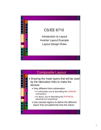
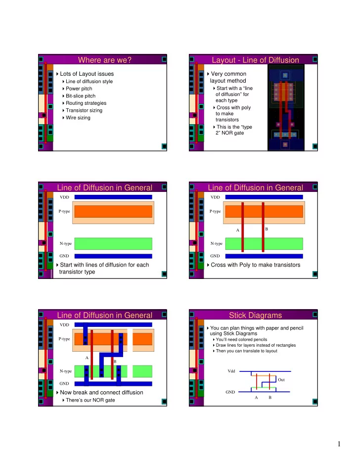
Where are we? Layout - Line of Diffusion � Lots of Layout issues � Very common layout method � Line of diffusion style � Start with a “line � Power pitch of diffusion” for � Bit-slice pitch each type � Routing strategies � Cross with poly � Transistor sizing to make � Wire sizing transistors � This is the “type 2” NOR gate Line of Diffusion in General Line of Diffusion in General VDD VDD P-type P-type B A N-type N-type GND GND � Start with lines of diffusion for each � Cross with Poly to make transistors transistor type Line of Diffusion in General Stick Diagrams VDD � You can plan things with paper and pencil using Stick Diagrams P-type � You’ll need colored pencils � Draw lines for layers instead of rectangles � Then you can translate to layout A B N-type Vdd Out GND � Now break and connect diffusion GND A B � There’s our NOR gate 1
Gate Layout Example: Inverter � Layout can be very time consuming � Design gates to fit together nicely � Build a library of standard cells � Standard cell design methodology � V DD and GND should abut (standard height) � Adjacent gates should satisfy design rules � nMOS at bottom and pMOS at top � All gates include well and substrate contacts Example: NAND3 Stick Diagrams � Horizontal N-diffusion and p-diffusion � Stick diagrams help plan layout quickly strips � Need not be to scale � Vertical polysilicon gates � Draw with color pencils or dry-erase markers � Metal1 V DD rail at top � Metal1 GND rail at bottom � 32 λ by 40 λ Wiring Tracks Well spacing � Wells must surround transistors by 6 λ � A wiring track is the space required for a � Implies 12 λ between opposite transistor wire � 4 λ width, 4 λ spacing from neighbor = 8 λ flavors pitch � Leaves room for one wire track � Transistors also consume one wiring track 2
Area Estimation Example: O3AI � Estimate area by counting wiring tracks � Sketch a stick diagram for O3AI and � Multiply by 8 to express in λ estimate area ( ) � = + + Y A B C D Example: O3AI Example: O3AI � Sketch a stick diagram for O3AI and � Sketch a stick diagram for O3AI and estimate area estimate area ( ) = + + ( ) � � = + + Y A B C D Y A B C D Euler Paths Simple example: NOR Vdd Vdd � A graphical method for planning complex A Vdd A 1 gate layout A 1 GND B Out B � Take the transistor netlist and draw it as a 1 Out graph Out B � Note that the pull-up and pull-down trees Out A B A B can be duals of each other � Find a path that traverses the graph with the GND GND same variable ordering for pull-up and pull- � Euler path is a tour of all edges down graphs � Find a path that has the same ordering for pull-up and � This guides you to a line of diffusion layout pull-down, I.e. A B � Vdd A 1 B Out GND A Out B GND 3
This Path Translates to Layout Examples � Find a path that has the same ordering for pull- � Switch to chalkboard for examples up and pull-down, I.e. A B � Also chalkboard examples of latches and � You can also include all the internal nodes � Pull-up: Vdd A 1 B Out feedback � Pull-Down: GND A Out B GND � Line of diffusion layout Vdd Out GND A B Layout Example: Flip Flop Zoom in on Latch � Simple D-type edge triggered flip flop � Need two copies of this for a full D flip flop Stick Diagram of Latch Stick Diagram of Latch � First add the gates � First add the gates � Note where outputs can be shared � Note where outputs can be shared � Ignore details of signal crossings for now… � Ignore details of signal crossings for now… 1 2 1 2 4
Stick Diagram of Latch Stick Diagram of Latch � First add the gates � First add the gates � Note where the signals are relative to the schematic � Note where the signals are relative to the � Note where additional connections are needed schematic 2 2 1 1 D D C Cb C Cb 1 2 1 2 Start With First Enabled Inv Add Next Enabled Inverter � Add two more poly � I’m using 5u power gates for second wires, 29u vertical enabled inverter picth based on the � Note that the two C5x standard cell enabled inverters share model an output (not connected � Probably overkill… yet) � Add DIF for N- and � Note that I’ve added P-type transistors vdd! and gnd! For DRC � Note 2x standard � I’ll deal with C-Cb size because of crossover later… serial connection Aside: Multiple Contacts Contact Option #1 � Total equivalent resistance = 56.1 Ohms � Metal resistance = 0.05 O/square � Contact resistance = 5 O/contact � Active resistance = 70 O/square � Gate resistance = 50 O/square � Look at a model of transistor resistance � Active resistance 7O - contact to gate 5
Contact Option #2 Contact Option #3 � Total equivalent resistance = 24.7 Ohms � Total equivalent resistance = 105.1 Ohms � So, put in as many contacts as will fit along side a wide gate… Meanwhile, Add inverter Finish Inverter (mostly) � Note that it’s back � Make inverter to standard size output connections � Shares vdd/gnd � Don’t connect yet connection with � I’m going to use M1 enabled inverter as a horizontal � Minimum spacing layer for all transistors so � Which means far being careful about vertical use of M1 � Incremental DRC at EVERY step! Make Feedback Connections Deal With C/Cb Crossover � Start by cutting the � Output of inverter Cb C “select” gates of the (connected in M1 for enabled inverters now) goes to input of 2 nd enabled inverter � Output of enabled inverters goes to input 1 of inverter 2 � Note that outputs of D enabled inverters goes through POLY 1 2 C Cb 6
Connect the C Input Look at Gap � Prepare for M1 � You need to have enough space for crossover in C wire Cb C minimum width poly to fit through gap � C is N-type in first enabled inverter, P-type in second enabled inverter � Use M1PLY contacts � PROBLEM! We need to squeeze a poly wire inbetween those contacts… � Use design rules to plan C Cb for space Start Making Room � Jog the poly around � Push D-signal poly out and through the gap of the way with with minimum spacing minimum spacing to DIF to M1PLY contact on � We’ll move it back later both sides � Make sure to continue to DRC at every step! Fit Things Back Together � Now put big D-poly jog � Add M1PLY contacts for back as close as you can future connections � Need to get Cb, C, D signals into the latch in the future � Those will most likely be routed on some type of metal � So we need the M1 metal connection at the bottom 7
Plan For Clock Routing Bit Slice Plan � Break M1 output � Plan is to stitch these together to make a connection on inverter to register leave room for horizontal � Inputs on top in M2 M1 routing � Outputs on bottom in M2 � Clock and Clock-bar routed horizontally in M1 � I’ll eventually route C and Cb through the cell horizontally on M1 D2 D1 D0 D Vdd Vdd C Cb C Vss Qb2 Q2 Qb1 Q1 Qb0 Q0 Cb Vss Qb Q Need Second Latch Expand from Latch to F/F � Basically a copy of the first latch � Select and � But with reversed C and Cb connections copy the first � Copy the first layout… latch � Now I need to reverse the C and Cb connections C/Cb Routing Plan C/Cb Routing Plan � Remember � Remember my C/Cb my C/Cb routing plan routing plan � Plan for � Plan for where those where those wires can go wires can go 8
Connect Clocks to 1 st Latch Connect Clocks to 2nd Latch � Adjust contact � Now shift the positions for contacts the the first other way for enabled the second inverter latch � Makes the complementar y C/Cb connection Connect Clocks to 2 nd Latch Connect the Two Latches � Q of first goes � Now shift the to D of second contacts the other way for � Don’t really the second need both top latch and bottom � Makes the connections, complementary but it doesn’t C/Cb hurt connection � Lower resistance paths Note Extra Routing Channels Now Consider Output Inverters � Two more inverters � Note that this � Make them 2x size for output drive vertical pitch, and this cell contents have left two additional M1 horizontal routing channels through the middle of the cell 9
Output Inverters Make Output Connections � Add the DIF � Add vdd, gnd and for the output output contacts inverters � Add poly � Remember gates I want to � Make output make them connections 2x size in M2 � Connect to 2 nd latch and to 2 nd inverter Now Squeeze Inverter Keep Squeezing � Select regions of � Now the layout squeeze and stretch power to move it supply all to a new spot contacts Squeezed Version Final D-Type Flip Flop � Squeeze � Output vertically inverters since I don’t squeezed need extra together routing channels, � Note that D, and I don’t Q, And Qb are need to routed match with standard vertically in cells M2 � Add long TUB and SUB contacts 10
Put Four of them Together Zoom in to Cell Boundary D3 D2 D1 D0 C Q3 Q2 Q1 Q0 Cb � Add instances that abut � Or use the “array” feature of the instance dialog � There’s a little extra space � Note that C and Cb are routed in � Caused by wanting each latch to DRC on its own horizontal M1 � Could close this up by overlapping cells 11
Recommend
More recommend
Explore More Topics
Stay informed with curated content and fresh updates.
