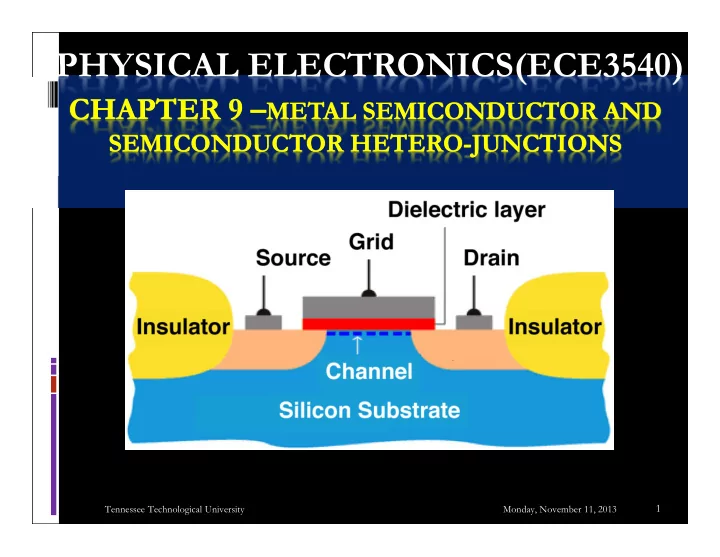
PHYSICAL ELECTRONICS(ECE3540) CHAPTER 9 METAL SEMICONDUCTOR AND - PowerPoint PPT Presentation
PHYSICAL ELECTRONICS(ECE3540) CHAPTER 9 METAL SEMICONDUCTOR AND CHAPTER 9 METAL SEMICONDUCTOR AND SEMICONDUCTOR HETERO-JUNCTIONS SEMICONDUCTOR HETERO-JUNCTIONS 1 Tennessee Technological University Monday, November 11, 2013 Brook Abegaz
PHYSICAL ELECTRONICS(ECE3540) CHAPTER 9 – METAL SEMICONDUCTOR AND CHAPTER 9 – METAL SEMICONDUCTOR AND SEMICONDUCTOR HETERO-JUNCTIONS SEMICONDUCTOR HETERO-JUNCTIONS 1 Tennessee Technological University Monday, November 11, 2013 Brook Abegaz
Introduction Chapter 4 : we considered the semiconductor in equilibrium and determined electron and hole concentrations in the conduction and valence bands, respectively. The net flow of the electrons and holes in a semiconductor generates current . The process by which these charged particles move is called transport . Chapter 5 : we considered the two basic transport mechanisms in a semiconductor crystal: drift: the movement of charge due to electric fields, and diffusion: the flow of charge due to density gradients. 2 Tennessee Technological University Monday, November 11, 2013
Introduction Chapter 6 : we discussed the behavior of non- equilibrium electron and hole concentrations as functions of time and space. We developed the ambi-polar transport equation which describes the behavior of the excess electrons and holes. Chapter 7 : We considered the situation in which a p-type and an n-type semiconductor are brought into contact with one another to form a PN junction. 3 Tennessee Technological University Monday, November 11, 2013
Introduction Chapter 8 : We considered the PN junction with a forward-bias applied voltage and determined the current-voltage characteristics. When holes flow from the p region across the space charge region into the n region, they become excess minority carrier holes and are subject to excess minority carrier diffusion, drift, and recombination. When electrons from the n region flow across the space charge region into the p region, they become excess minority carrier electrons and are subject to these same processes. 4 Tennessee Technological University Monday, November 11, 2013
Introduction When a sufficiently large reverse-bias voltage is applied across a PN junction, breakdown can occur, producing a large reverse-bias current in the junction, which can cause heating effects and catastrophic failure of the diode. Zener diodes are designed to operate in the breakdown region. Breakdown puts limits on the amount of voltage that can be applied across a PN junction. 5 Tennessee Technological University Monday, November 11, 2013
Introduction Chapter 9 : we will consider the metal- semiconductor junction and the semiconductor hetero-junction, in which the material on each side of the junction is not the same. These junctions can also produce diodes. An Ohmic contact is a low-resistance junction providing current conduction in both directions. We will examine the conditions that yield metal- semiconductor Ohmic contacts. 6 Tennessee Technological University Monday, November 11, 2013
Metal-Semiconductor Junction There are two kinds of metal-semiconductor contacts: Rectifying Schottky diodes: metal on lightly doped Silicon. Low-resistance Ohmic contacts: metal on heavily doped Silicon. 7 Tennessee Technological University Monday, November 11, 2013
The Schottky Barrier Diode Rectifying contacts are mostly made of n-type semiconductors; for this reason we will concentrate on this type of diode. In the ideal energy-band diagram for a particular metal and n- type semiconductor, the vacuum level is used as a reference. The parameter M is the metal work function (in volts), s is the semiconductor work function, and is known as the electron affinity. Before contact, the Fermi level in the semiconductor was above that in the metal. In order for the Fermi level to become a constant through the system in thermal equilibrium, electrons from the semiconductor flow into the lower energy states in the metal. 8 Tennessee Technological University Monday, November 11, 2013
The Schottky Barrier Diode The parameter B0 is the ideal barrier height of the semiconductor contact, the potential barrier seen by electrons in the metal trying to move into the semiconductor. The barrier is known as the Schottky barrier and is given as: ( ) 0 B M On the semiconductor side, is the built-in potential barrier. This barrier, similar to the case of the PN Junction, is the barrier seen by electrons in the conduction band trying to move into the metal V bi is given as: ( ) V 0 bi B n 9 Tennessee Technological University Monday, November 11, 2013
The Schottky Barrier Diode Bn Increases with Increasing Metal Work Function Vacuum level, E 0 M Si = 4.05 eV : Work Function q M of metal Si : Electron Affinity of Si q Bn E c E f Theoretically, Bn = M – Si E v x = 0 x = x n Fig. 9.1: Ideal energy-band diagram of a metal-semiconductor junction 10 Tennessee Technological University Monday, November 11, 2013
The Schottky Barrier Diode Depletion Metal Neutral region layer q Bn E c • Schottky barrier height, B , E f is a function of the metal N-Si material. E v • B is the most important E c parameter. The sum of q Bn P-Si and q Bp is equal to E g . E f q Bp E v Fig. 9.2: Energy Band Diagram of Schottky Contact 11 Tennessee Technological University Monday, November 11, 2013
The Schottky Barrier Diode Schottky barrier heights for electrons and holes Metal Mg Ti Cr W Mo Pd Au Pt Bn (V) 0.4 0.5 0.61 0.67 0.68 0.77 0.8 0.9 Bp (V) 0.61 0.5 0.42 0.3 Work Function 3.7 4.3 4.5 4.6 4.6 5.1 5.1 5.7 m (V) Bn + Bp E g Bn increases with increasing metal work function 12 Tennessee Technological University Monday, November 11, 2013
The Schottky Barrier Diode • A high density of energy Vacuum level, E 0 states in the band gap at Si = 4.05 eV the metal-semiconductor q M interface pins E f to a narrow range and Bn is q Bn E c typically 0.4 to 0.9 V + E f • Question: What is the typical range of Bp ? E v Fig. 9.3: Fermi Level Pinning 13 Tennessee Technological University Monday, November 11, 2013
The Schottky Barrier Diode Schottky Contacts of Metal Silicide on Si Silicide: A Silicon and metal compound. It is conductive similar to a metal. Silicide-Si interfaces are more stable than metal-silicon interfaces. After metal is deposited on Si, an annealing step is applied to form a Silicide-Si contact. The term metal-silicon contact includes and almost always means Silicide-Si contacts. Silicide ErSi 1.7 HfSi MoSi 2 ZrSi 2 TiSi 2 CoSi 2 WSi 2 NiSi 2 Pd 2 Si PtSi f Bn (V) 0.28 0.45 0.55 0.55 0.61 0.65 0.67 0.67 0.75 0.87 f Bp (V) 0.55 0.49 0.45 0.45 0.43 0.43 0.35 0.23 Table. 9.1: Schottky Contacts of Metal Silicide on Si 14 Tennessee Technological University Monday, November 11, 2013
The Schottky Barrier Diode ( ) qV q E E q bi q Bn bi Bn c f E c N E f c ln q kT Bn N d 2 ( ) V V E v s bi R W x dep n qN d q Bn q( bi + V) eN x s d n | | C A E max W qV dep s E c Question: E f How should we plot the CV data to extract bi ? E v Fig. 9.4: Using C-V Data to Determine B 15 Tennessee Technological University Monday, November 11, 2013
Exercise 1. Consider a contact between Tungsten and an n-type Silicon doped to N d = 10 16 cm -3 at T = 300K. Calculate the theoretical barrier height, built-in potential barrier and maximum electric field in the metal-semiconductor diode for a zero applied bias. Use the metal work function for Tungsten as M = 4.55V and electron affinity for Silicon = 4.01V. ( ) V ( ) 0 bi B n 0 B M eN d x 2 ( ) V V | | n E s bi R W x max dep n qN s d 16 Tennessee Technological University Monday, November 11, 2013
Solution B0 is the ideal Schottky barrier height. ( ) 4 . 55 4 . 01 0 . 54 V 0 B M The space charge width at a zero bias is: 19 2 . 8 10 kT N x c ln 0 . 0259 ln 0 . 206 V n 16 10 e N d ( ) 0 . 54 0 . 206 0 . 33 V V 0 bi B n 14 2 ( ) 2 ( 11 . 7 )( 8 . 85 * 10 )( 0 . 33 ) V V - 4 s bi R 0.207 * 10 cm W x dep n 19 16 ( 1 . 6 * 10 )( 10 ) qN d 19 16 4 ( 1 . 6 * 10 )( 10 )( 0 . 207 * 10 ) eN x 4 d n | | 3 . 2 * 10 / E V cm max 14 ( 11 . 7 )( 8 . 85 * 10 ) s 17 Tennessee Technological University Monday, November 11, 2013
The Schottky Barrier Diode Using CV Data to Determine B 1 2 ( ) V bi 2 2 C qN A d s 2 1/C q bi q Bn E c E f V E bi v Fig. 9.5: Using C-V Data to Determine C 18 Tennessee Technological University Monday, November 11, 2013
Recommend
More recommend
Explore More Topics
Stay informed with curated content and fresh updates.
