PHYSICAL ELECTRONICS(ECE3540) CHAPTER 4 THE SEMICONDUCTOR IN - PowerPoint PPT Presentation
PHYSICAL ELECTRONICS(ECE3540) CHAPTER 4 THE SEMICONDUCTOR IN EQUILIBRIUM Brook Abegaz, Tennessee Technological University, Fall 2013 1 Tennessee Technological University Friday, September 20, 2013 Chapter 4 The Semiconductor in
PHYSICAL ELECTRONICS(ECE3540) CHAPTER 4 – THE SEMICONDUCTOR IN EQUILIBRIUM Brook Abegaz, Tennessee Technological University, Fall 2013 1 Tennessee Technological University Friday, September 20, 2013
Chapter 4 – The Semiconductor in Equilibrium Chapter 3: considering a general crystal and applying to it the concepts of quantum mechanics in order to determine a few of the characteristics of electrons in a single-crystal lattice. Chapter 4: apply these concepts specifically to a semiconductor material. Chapter 4: use the density of quantum states in the conduction band and the density of quantum states in the valence band along with the Fermi-Dirac probability function to determine the concentration of electrons and holes in the conduction and valence bands 2 Tennessee Technological University Friday, September 20, 2013
Chapter 4 – The Semiconductor in Equilibrium Equilibrium, or thermal equilibrium, implies that no external forces such as voltages, electric fields, magnetic fields, or temperature gradients are acting on the semiconductor. All properties of the semiconductor will be independent of time in this case. An intrinsic semiconductor = a pure crystal with no impurity atoms or defects. The electrical properties of an intrinsic semiconductor can be altered in desirable ways by adding controlled amounts of specific impurity atoms, called dopant atoms, to the crystal, thus creating an extrinsic semiconductor. Adding dopant atoms changes the distribution of electrons among the available energy states, so the Fermi energy becomes a function of the type and concentration of impurity atoms. 3 Tennessee Technological University Friday, September 20, 2013
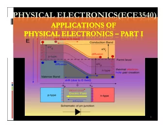
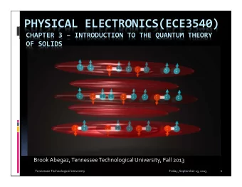
Chapter 4 – The Semiconductor in Equilibrium Fig. 1: Thermal Excitation caused jumping of an electron to CB. There is a corresponding hole created in VB where the electron was located. 4 Tennessee Technological University Friday, September 20, 2013
Charge Carriers in Semiconducductors Current is the rate at which charge flows. In a semiconductor, two types of charge carriers, the electron and the hole, can contribute to a current. Since the current in a semiconductor is determined largely by the number of electrons in the conduction band and the number of holes in the valence band, an important characteristics is the density of these charge carriers. 5 Tennessee Technological University Friday, September 20, 2013
Equilibrium Distribution of Electrons and Holes The distribution (with respect to energy) of electrons in the conduction band is given by the density of allowed quantum states times the probability that a state is occupied by an electron. eq. (4.1) n(E) = g (E) f (E) c F where f F (E) is the Fermi-Dirac probability function and g c (E) is the density of quantum states in the conduction band. The total electron concentration per unit volume in the conduction band is then found by integrating Equation (4.1) over the entire conduction-band energy. 6 Tennessee Technological University Friday, September 20, 2013
Equilibrium Distribution of Electrons and Holes The distribution (with respect to energy) of holes in the valence bend is the density of allowed quantum states in the valence hand multiplied by the probability that a state is not occupied by an electron. eq. (4.2) p(E) = g (E)[1 - f (E)] v F The total hole concentration per unit volume is found by integrating this function over the entire valence-band energy. 7 Tennessee Technological University Friday, September 20, 2013
Equilibrium Distribution of Electrons and Holes An ideal intrinsic semiconductor is a pure semiconductor with no impurity atoms and no lattice defects in the crystal (e.g. pure Silicon). For an intrinsic semiconductor at T = 0K, all energy states in the valence band are filled with electrons and all energy states in the conduction band are empty of electrons. The Fermi energy must, therefore, be somewhere between E c and E v (The Fermi energy does not need to correspond to an allowed energy.) 8 Tennessee Technological University Friday, September 20, 2013
The n o and p o Equations The equation for the thermal-equilibrium concentration of electrons may be found by integrating Equation (4.1) over the conduction band energy, as: n g ( E ) f ( E ) dE 0 c F eq. (4.3) Applying the Boltzmann approximation to the Fermi energy calculation, the thermal-equilibrium density of electrons in the conduction band is: eq. (4.4) * 3 / 2 4 ( 2 m ) ( E E ) n F ( ) exp[ ] n E E dE 0 c 3 h kT E c 9 Tennessee Technological University Friday, September 20, 2013
The n o and p o Equations Solving the integral, substitute N c as the effective density of states function in the conduction band. * 2 m kT eq. (4.5) 3 / 2 n N 2 ( ) c 2 h If m* = m o , then the value of the effective density of states function at T = 300 K is N c = 2.5 x 10 19 cm -3 , which is the value of N c for most semiconductors. If the effective mass of the electron is larger or smaller than m o , then the value of the effective density of states function changes accordingly, but is still of the same order of magnitude. The thermal-equilibrium electron concentration in the conduction band is: eq. (4.6) ( E E ) c F n N exp[ ] 0 c kT 10 Tennessee Technological University Friday, September 20, 2013
The n o and p o Equations The thermal-equilibrium concentration of holes in the valence band is found by integrating Equation (4.2) over the valence band energy as: eq. (4.7) ( )[ 1 ( )] p g E f E dE 0 v F 1 eq. (4.8) 1 f ( E ) F E E F 1 exp( ) kT Defining the effective density of states function in the valence band: * 2 m kT p 3 / 2 eq. (4.9) N 2 ( ) v 2 h The thermal-equilibrium concentration of holes in the valence band is then: eq. (4.10) ( E E ) F v p N exp[ ] 0 v kT 11 Tennessee Technological University Friday, September 20, 2013
The n o and p o Equations The effective density of states functions, N c and N v are constant for a given semiconductor material at a fixed temperature. The values of the density of states function and of the effective masses for Silicon, Gallium Arsenide, and Germanium are: Table 4.1 Effective Density of States Function and Effective Mass Values N c (cm ‐ 3 ) N v (cm ‐ 3 ) * /m 0 * /m 0 m n m p 2.8*10 19 1.04*10 19 Silicon 1.08 0.56 Gallium Arsenide 4.7*10 17 7.0*10 18 0.067 0.48 1.04*10 19 6.0*10 18 Germanium 0.55 0.37 The thermal equilibrium concentrations of electrons in the conduction band and of holes in the valence band are directly related to the effective density of states constants and to the Fermi energy level. 12 Tennessee Technological University Friday, September 20, 2013
The Intrinsic Carrier Concentration For an intrinsic semiconductor, the concentration of electrons in the conduction band (n) is equal to the concentration of holes in the valence band (p). These parameters are usually referred to as the intrinsic electron concentration (n i ) and intrinsic hole concentration (p i ). The Fermi energy level for the intrinsic semiconductor is called the intrinsic Fermi energy, or E f = E fi . 13 Tennessee Technological University Friday, September 20, 2013
The Intrinsic Carrier Concentration For an intrinsic semiconductor: eq. (4.11) ( E E ) c Fi n n N exp[ ] 0 i c kT eq. (4.12) ( E E ) Fi v p p n N exp[ ] 0 i i v kT eq. (4.13) ( E E ) ( E E ) 2 c Fi Fi v n N N exp[ ] . exp[ ] i c v kT kT eq. (4.14) ( E ) ( E E ) 2 g c v n N N exp[ ] N N exp[ ] i c v c v kT kT 14 Tennessee Technological University Friday, September 20, 2013
The Intrinsic Carrier Concentration For a given semiconductor material at a constant temperature, the value of n i is a constant, and independent of the Fermi energy. Table 4.2 Commonly Accepted Values of n i at T=300K n i (cm -3 ) 1.5*10 10 Silicon 1.8*10 6 Gallium Arsenide 2.4*10 13 Germanium Fig. 2: Intrinsic carrier concentration n i with respect to change in T o . 15 Tennessee Technological University Friday, September 20, 2013
Application of Intrinsic Semiconductors High Electron Mobility Transistor High resistivity substrate for RF circuits Amorphous ‐ Si Solar Cells Fig. 3: Structure of a Solar Cell. 16 Tennessee Technological University Friday, September 20, 2013
The n o p o Product Using the general expressions for n o and p o : ( ) ( ) E E E E c F F v n p N N exp[ ] exp[ ] eq. (4.15) 0 0 c v kT kT which is simplified as: ( E ) g n p N N exp[ ] eq. (4.16) 0 0 c v kT Thus, for a semiconductor in thermal equilibrium, the Mass Action Law states: eq. (4.17) 2 n p n 0 0 i 17 Tennessee Technological University Friday, September 20, 2013
Recommend
More recommend
Explore More Topics
Stay informed with curated content and fresh updates.
