PHYSICAL ELECTRONICS(ECE3540) CHAPTER 5 CARRIER TRANSPORT - PowerPoint PPT Presentation
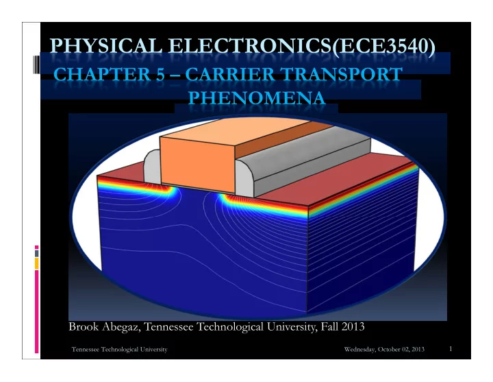
PHYSICAL ELECTRONICS(ECE3540) CHAPTER 5 CARRIER TRANSPORT PHENOMENA Brook Abegaz, Tennessee Technological University, Fall 2013 1 Tennessee Technological University Wednesday, October 02, 2013 Chapter 5 Carrier Transport Phenomena
PHYSICAL ELECTRONICS(ECE3540) CHAPTER 5 – CARRIER TRANSPORT PHENOMENA Brook Abegaz, Tennessee Technological University, Fall 2013 1 Tennessee Technological University Wednesday, October 02, 2013
Chapter 5 – Carrier Transport Phenomena Chapter 4 : we considered the semiconductor in equilibrium and determined electron and hole concentrations in the conduction and valence bands, respectively. The net flow of the electrons and holes in a semiconductor will generate currents . The process by which these charged particles move is called transport . Chapter 5 : we will consider the two basic transport mechanisms in a semiconductor crystal: drift the movement of charge due to electric fields, and diffusion the flow of charge due to density gradients. 2 Tennessee Technological University Wednesday, October 02, 2013
Carrier Drift An electric field applied to a semiconductor will produce a force on electrons and holes so that they will experience a net acceleration and net movement, provided there are available energy states in the conduction and valence hands. This net movement of charge due to an electric field is called drift. The net drift of charge gives rise to a drift current . Dr Drift ift Curr urrent nt Density Density : for a positive volume charge density p moving at an average drift velocity v d , the drift current density is given by: J v drf d where J is in units of C/cm 2 -s or amps/cm 2 . 3 Tennessee Technological University Wednesday, October 02, 2013
Carrier Drift If the volume charge density is due to positively charged holes, then : ( ) J ep v | | p drf d p where J p|drf is the drift current density due to holes and v d|p is the average drift velocity of the holes. The equation of motion of a positively charged hole in the presence of an electric field is: * F m a eE p where e is the magnitude of the electronic charge, a is the * is the effective mass of acceleration, E is the electric field, and m p the hole. If the electric field is constant, then we expect the velocity to increase linearly with time. However, charged particles in a semiconductor are involved in collisions with ionized impurity atoms and with thermally vibrating lattice atoms. These collisions, or scattering events, alter the velocity characteristics of the particle. 4 Tennessee Technological University Wednesday, October 02, 2013
Carrier Drift As the hole accelerates in a crystal due to the electric field, the velocity increases. When the charged particle collides with an atom in the crystal, the particle loses most or all of its energy. The particle will again begin to accelerate and gain energy until it is again involved in a scattering process. Throughout this process, the particle will gain an average drift velocity which, for low electric fields, is directly proportional to the electric field. We may then write v E dp p where p, is the proportionality factor and is called the hole mobility. The mobility of a semiconductor describes how well a particle will move due to an electric field. The unit of mobility is expressed in terms of cm 2 /V-s. By combining the above equations, we may write the drift current density due to holes as ( ) J ep v e pE | p drf dp p The drift current due to holes is in the same direction as the applied electric field. The same discussion of drift applies to electrons. ( ) ( ) J ep v en v | n drf dn dn Where J n|drf is the drift current density due to electrons and v dn is the average drift velocity of electrons. The net charge density of electrons is negative. 5 Tennessee Technological University Wednesday, October 02, 2013
Carrier Drift The average drift velocity of an electron is also proportional to the electric field for small fields. However, since the electron is negatively charged, the net motion of the electron is opposite to the electric field direction. Therefore, v E dn n where μ n is the electron mobility and is a positive quantity. ( )( ) J en E e nE | n drf n n The conventional drift current due to electrons is also in the same direction as the applied electric field even though the electron movement is in the opposite direction. Electron and hole mobilities are functions of temperature and doping concentrations. Since both electrons and holes contribute to the drift current, the total drift current is the sum of the individual electron and hole drift current densities, therefore: ( ) J e n p E drf n p 6 Tennessee Technological University Wednesday, October 02, 2013
Exercise 1. Consider a Gallium Arsenide sample which is at T = 300K and with doping concentrations of N a =10cm -3 and N d = 10 16 cm -3 . Assume a complete ionization and assume electron and hole mobilities given in Table 5.1. Calculate the drift current density if the applied electric field is E = 10V/cm 2 . 7 Tennessee Technological University Wednesday, October 02, 2013
Solution 1. Using the formula: ( ) N N N N 2 2 16 3 d a ( d a ) 10 n n cm i 2 2 The minority carrier hole concentration is: 2 6 2 ( 1 . 8 * 10 ) n 4 3 i 3 . 24 * 10 p cm 16 ( 1 * 10 ) n The drift current density for this extrinsic n- type semiconductor is: A ( ) ( ) 136 J e n p E e N E drf n p n d 2 cm 8 Tennessee Technological University Wednesday, October 02, 2013
Mobility Effects Mobility relates the average drift velocity of a carrier to the electric field. dv * F m eE p dt where v is the velocity of the particle due to the electric field and does not include the random thermal velocity. eEt ( ) v J e n p E * drf n p m p In a random thermal velocity and motion of a hole in a semiconductor with zero electric field, there is a mean time between collisions, denoted by cp . If a small electric field is applied, there will be a net drift of the hole in the direction of the E-field, and the net drift velocity will be a small perturbation on the random thermal velocity, so the time between collisions will not be altered appreciably. e cp ( ) v E d | peak * m p 9 Tennessee Technological University Wednesday, October 02, 2013
Mobility Effects The average drift velocity is one half the peak value: 1 e cp ( ) v E d * 2 m p Statistically, the hole mobility and the electron mobility are given as: e v e dp cp cn p n * * E m m p n where n is the mean time between collisions for an electron. There are two collision or scattering mechanisms that dominate in a semiconductor and affect the carrier mobility: phonon or lattice scattering and ionized impurity scattering. 10 Tennessee Technological University Wednesday, October 02, 2013
Phonon or Lattice Scattering The atoms in a semiconductor crystal have a certain amount of thermal energy at temperatures above absolute zero that causes the atoms to randomly vibrate about their lattice position within the crystal. The lattice vibrations cause a disruption in perfect periodic potential function. A perfect periodic potential in a solid allows electrons to move unimpeded, or with no scattering, through the crystal. Thermal vibrations however cause a disruption of the potential function, resulting in an interaction between the electrons or holes and the vibrating lattice atoms. This lattice scattering is also referred to as phonon scattering. Since lattice scattering is related to the thermal motion of atoms, the rate at which the scattering occurs is a function of temperature. If we denote μ L as the mobility observed if only lattice scattering existed, then the scattering theory states the relation to first order: 3 L 2 T 11 Tennessee Technological University Wednesday, October 02, 2013
Ionized Impurity Scattering Impurity atoms are added to the semiconductor to control or alter its characteristics. These impurities are ionized at room temperature so that a Coulomb interaction exists between the electrons or holes and the ionized impurities. This coulomb interaction produces scattering or collisions and also alters the velocity characteristics of the charge carrier. If we denote μ I as the mobility that would be observed if only ionized impurity scattering existed, then: 3 2 T I + + N a N - is the total ionized impurity I where N I = N d concentration in the semiconductor. 12 Tennessee Technological University Wednesday, October 02, 2013
Ionized Impurity Scattering If temperature increases, the random thermal velocity of a carrier increases, reducing the time the carrier spends in the vicinity of the ionized impurity 3 center. 2 T I N I The less time spent in the vicinity of a coulomb force, the smaller the scattering effect and the larger the expected value of μ I . If the number of ionized impurity centers increases, then the probability of a carrier encountering an ionized impurity center increases, implying a smaller value of μ I . 13 Tennessee Technological University Wednesday, October 02, 2013
Recommend
More recommend
Explore More Topics
Stay informed with curated content and fresh updates.
