Outline Introduction neering Composite Materials Design with - PDF document
12/4/2010 Cullen College of Engineering University of Houston Design/Modeling for Periodic neering trical & Computer Engin N Nano Structures for EMC/EMI St t f EMC/EMI Ji Chen Elect Department of Electrical and Computer Engineering
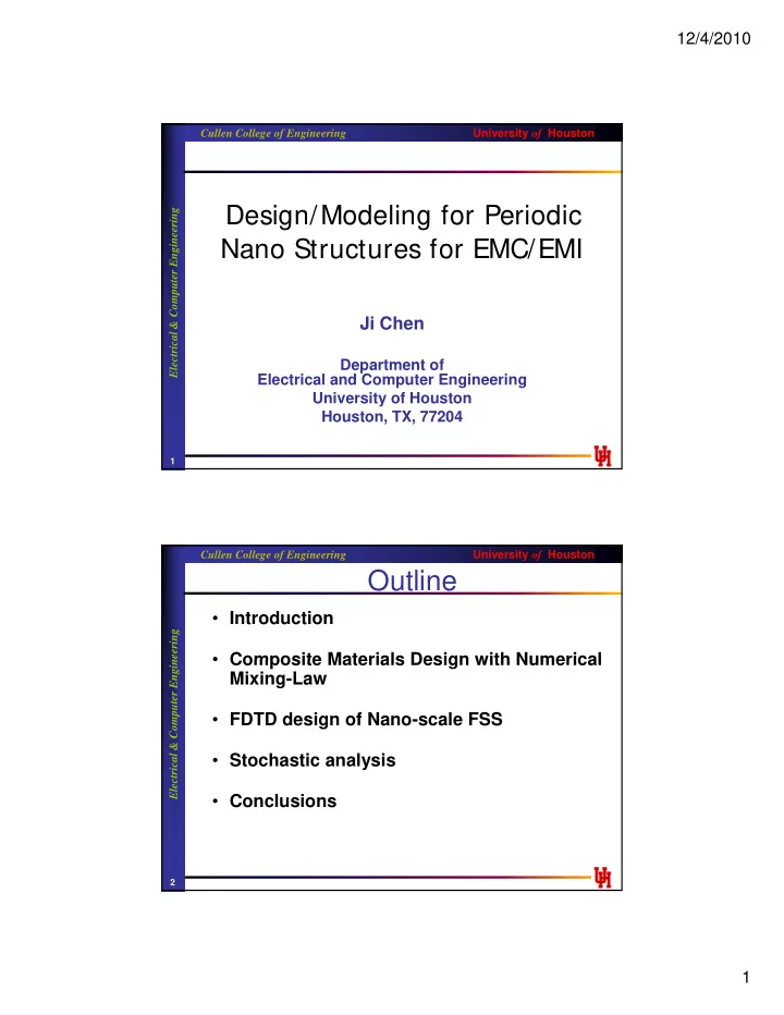
12/4/2010 Cullen College of Engineering University of Houston Design/Modeling for Periodic neering trical & Computer Engin N Nano Structures for EMC/EMI St t f EMC/EMI Ji Chen Elect Department of Electrical and Computer Engineering University of Houston Houston, TX, 77204 1 Cullen College of Engineering University of Houston Outline • Introduction neering • Composite Materials Design with Numerical • Composite Materials Design with Numerical trical & Computer Engin Mixing-Law • FDTD design of Nano-scale FSS • Stochastic analysis Elect • Conclusions 2 1
12/4/2010 Cullen College of Engineering University of Houston Introduction Electromagnetic Compatibility /Electromagnetic Interference neering trical & Computer Engin Elect http://en.wikipedia.org/wiki/Electromagnetic_compatibility 3 Cullen College of Engineering University of Houston Shielding neering trical & Computer Engin Elect NASA JSC Nanotube http://research.jsc.nasa.gov/BiennialResearchReport/PDF/Eng-8.pdf http://www.ursi.org/Proceedings/ProcGA05/pdf/E01.3(01681).pdf 4 2
12/4/2010 Cullen College of Engineering University of Houston Shielding Materials with Periodic Structures neering trical & Computer Engin 450nm length 650nm Pitch 100nm Arm s Elect FSS 5 Cullen College of Engineering University of Houston Composite Materials with Numerical Mixing-Law neering trical & Computer Engin Maxwell-Garnett equation q Elect ε − ε N ∑ k e f ε − ε + 3 3 ( ) a / a L k ε + ε ε − ε + ε + ε 2 1 e 2 1 ( ) ( 2 ) ε = ε + ε = ε − ε ε + ε + k 1 k e 1 e 1 e 3 ( 2 ) L = ε − ε eff e 1 e eff e e f N ∑ ε + ε ε − ε + 3 3 − 2 ( ) a / a L k e ε + ε + ε − ε 1 f eff e 2 1 2 1 ( 2 ) 2 ( ) ε + ε ε + ε + k 1 e 1 e ( 2 ) L 2 = 2 1 k 1 k e 6 3
12/4/2010 Cullen College of Engineering University of Houston Composite Materials with Numerical Mixing-Law neering trical & Computer Engin 3D Periodical Structure Periodic Composite Material Elect Unit Element 7 Cullen College of Engineering University of Houston FDM FDM Zmax neering PBC Voltage V Voltage V trical & Computer Engin PBC Voltage Voltage PBC Xmax PBC Ymax PBC: periodic boundary condition PBC: periodic boundary condition Elect Unit Element 8 4
12/4/2010 Cullen College of Engineering University of Houston Effect of Effect of I Inclusion nclusion E Electrical lectrical P Properties roperties neering trical & Computer Engin Elect ε = l =1cm, 1, r _ host ε = ε = ε = 3, 1 rx inclusion _ ry inclusion _ rz inclusion _ 9 Cullen College of Engineering University of Houston Effect of Effect of I Inclusion nclusion E Electrical lectrical P Properties roperties neering trical & Computer Engin Elect ε ε = = l l =1cm, =1cm, 1, 1, r _ host r _ host ε ε = = ε ε = = ε ε = = 30 3 30, 3 , 3 1 rx inclusion rx inclusion _ _ ry inclusion ry _ _ inclusion rz rz _ _ inclusion inclusion 10 5
12/4/2010 Cullen College of Engineering University of Houston neering trical & Computer Engin Elect 11 Cullen College of Engineering University of Houston Electrical Properties Versus Frequency Electrical Properties Versus Frequency neering trical & Computer Engin Elect 12 6
12/4/2010 Cullen College of Engineering University of Houston Cubic Inclusion Cubic Inclusion neering trical & Computer Engin Vf=0.764 Elect 13 Cullen College of Engineering University of Houston Numerical Results Versus Frequency Numerical Results Versus Frequency neering trical & Computer Engin ε = ε × + ε × − V (1 V ) eff incl f host f Elect 14 7
12/4/2010 Cullen College of Engineering University of Houston Optimization for Multiphase Mixture neering trical & Computer Engin volume fractions 0.1. espr: 4.42 and 4.04 Elect Conductivity : 0.00715 S/m and 1.369 S/m 15 Cullen College of Engineering University of Houston FDTD Modeling neering trical & Computer Engin Elect 16 8
12/4/2010 Cullen College of Engineering University of Houston Challenge in the Modeling of IR FSSs Challenge in the Modeling of IR FSSs Lorentz-Drude Model (gold) � neering PEC assumption is not valid any more � The metal is highly frequency- ( ) ( ) ( ) ( ) ( ) ( ) ε ε ω ω = ε ε ω ω + + ε ε ω ω f f b dependent now dependent no trical & Computer Engin r r r � It has both negative permittivity ⎛ ⎞ ⎛ ⎞ Ω ω 2 2 and conductive loss k f ∑ − + ⎜ ⎟ ⎜ p ⎟ i p � = 1 ( ) But all of the tradition microwave ⎜ ( ) ⎟ ⎜ ⎟ ω ω − Γ ω − ω + ω Γ 2 2 ⎝ j ⎠ j designs are based on this ⎝ ⎠ = i 1 0 i i assumption. � FDTD Modeling for Periodic Structures Elect 17 Cullen College of Engineering University of Houston Finite-Sized Electromagnetic Source k x z z PBC PBC k z k 0 neering ? ? “Brute Force” …. …. …. …. trical & Computer Engin x a x a Plane Wave Incidence Finite Size Source Incidence � Plane wave incidence ( ) ( ) ( ) ( ) ⎡ + + ⎤ = ⎡ ⎤ e − jk a ⎣ E x a , H x a ⎦ ⎣ E x , H x ⎦ x Elect � Periodic boundary condition (PBC) can be applied for above equation in both frequency and time domains � Finite size source incidence � Assumption is no longer valid � In time domain, “Brute Force” FDTD simulation is needed 18 9
12/4/2010 Cullen College of Engineering University of Houston ASM-FDTD Method z + n z E tot x ( na y t , , ) n th unit cell neering …. …. …. …. trical & Computer Engin x x a a n =2 n =-2 n =-1 n =0 n =1 � Spectral domain transformation of the finite size source π ∞ / a ( ) a ( ) ( ) ∑ ( ) ( ) ( ) ∫ % − = % = δ − − δ − i i i i jk na J x , y J k dk J x y k , , J x , y x x na y y e x 0 0 π − x x x 0 0 0 0 2 π =−∞ / a n � The field in the 0th unit cell excited by this source can be represented as π / a a ∫ ∫ = 0 0 0 0 Elect E E ( , , ) ( x y t ) E E ( ( k k , , ) y t dk ) dk π − tot tot x x 2 π / a The 0 th unit cell spectral domain solution can be obtained by 0 ( � E k , , ) y t tot x FDTD simulation when following PBC is applied y t e − = 0 0 jk a E ( , , ) a y t E (0, , ) x tot tot π / a � a ∫ The field in n th cell is found by + = − n 0 jk na E ( x na y t , , ) E ( k , , ) y t e x dk tot π tot x x 2 − π / a 19 Cullen College of Engineering University of Houston Numerical Examples neering trical & Computer Engin dipole source 45 mm above the structure dipole source 45 mm above the structure Elect dipole strip 12 mm by 3 mm periodicity 15 mm in both directions field sampled 90 mm under the dipole source 20 10
12/4/2010 Cullen College of Engineering University of Houston Different Model Impacts On The Final Result Different Model Impacts On The Final Result neering trical & Computer Engin Elect Simulated transmission intensity of an Au cross slot array on the quartz substrate (a=650nm, L=500nm, W=110nm, thickness=300nm and substrate dielectric constant is 2.1316 21 Cullen College of Engineering University of Houston Three Practical Patterns I: Standard Case Three Practical Patterns I: Standard Case neering trical & Computer Engin Elect Simulated transmission intensity of an Au cross slot array on the quartz substrate (a=660nm, L=510nm, W=160nm, thickness=220nm and substrate dielectric constant is 2.1316 22 11
12/4/2010 Cullen College of Engineering University of Houston Five Practical Patterns II: Faced Centered Case Five Practical Patterns II: Faced Centered Case neering trical & Computer Engin Elect Simulated transmission intensity of an Au cross slot array on the quartz substrate (a=660nm, L=500nm, W=170nm, thickness=220nm and substrate dielectric constant is 2.1316 23 Cullen College of Engineering University of Houston Variation quantification � Composite mixtures have inherent randomness neering trical & Computer Engin � The homogenized EM property needs to be evaluated � Sources of randomness includes -- material electrical properties Elect -- component geometry 24 12
Recommend
More recommend
Explore More Topics
Stay informed with curated content and fresh updates.
