Opportunities and Challenges for Nanoelectronic Devices and - PowerPoint PPT Presentation
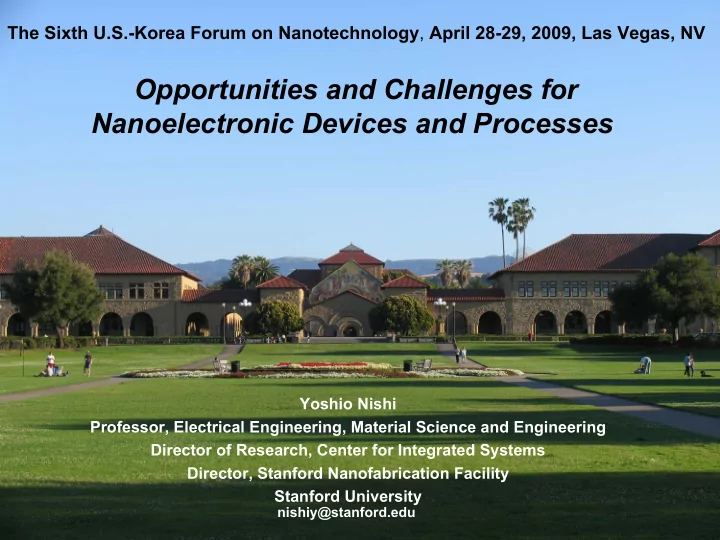
The Sixth U.S.-Korea Forum on Nanotechnology , April 28-29, 2009, Las Vegas, NV Opportunities and Challenges for Nanoelectronic Devices and Processes Yoshio Nishi Professor, Electrical Engineering, Material Science and Engineering Director of
The Sixth U.S.-Korea Forum on Nanotechnology , April 28-29, 2009, Las Vegas, NV Opportunities and Challenges for Nanoelectronic Devices and Processes Yoshio Nishi Professor, Electrical Engineering, Material Science and Engineering Director of Research, Center for Integrated Systems Director, Stanford Nanofabrication Facility Stanford University nishiy@stanford.edu
Status Quo for “ “Moore Moore” ” and and “ “More Moore More Moore” ” Status Quo for • CMOS Scaling is not coming to an end • 45 nm is happening • 32 nm well on its way • 22 nm will happen • Major ongoing transformation of scaling caused by power and power/density • End of frequency scaling of single core processor • No “10 GHz” microprocessor (with the ~100 W cooling limit) • System performance based on multi-low-power cores and accelerators • Move away from frequency scaling • How many “Moore” generations? • As long as we have affordable lithography G. Shahidi, IBM
Paradigm Shift: Hitting the Cooling Limit • Moving a high power chip to the next node (with limitation on cooling and maximum T rise), actually will slow it down Peak Frequency (100W/cm2 cooling @ max T 85C) 1400 With Performance Scaling 1300 50 W 40 W 1200 Performance 72 W 65 W 80 W 1100 50 W No Perf. scaling 1000 25 W 100 W (Only Shrink) 900 800 90nm 65nm 45nm 32nm 22nm Technology End of frequency scaling @ ~4 GHz (with 100 W cooling)?
System Performance from Multi-Cores 14 IBM ES9000 Prescott 12 Module Heat Flux(watts/cm 2 ) 10 Squadrons 8 IBM GP IBM 3090S 6 Pentium 4 4 IBM 3090 2 Merced IBM 370 Vacuum IBM 360 Pentium II(DSIP) 0 Performance Low-Power Bipolar CMOS Multi-Core Density NMOS / PMOS CMOS CMOS /CMOS 1950 1960 1970 1980 1990 2000 2010
“Beyond Moore” On-going Trends • Nanoelectronics: Ge, III-V channel to nanowire/nanotubes and more • Nano-bio/medical: Bio-sensing, imaging • Energy: nanowire solar, nanotube hydrogen storage • Environmental sensing: Sensor network, gaseous molecules sensing, ocean, air… • Fusion of nanoelectronics and nanomechanical: New switches and memories
Year Optimistic scenario 06 07 08 09 10 11 12 13 14 15 16 17 18 19 20 Strained channel New channel materials, Ge, III-V 65nm SOI , FD, UTB Nanowire devices/nanotubes 45nm Molecular devices 32nm Spintronics 22nm Flash 15nm 10nm PCRAM FERAM 7nm? 5nm? ReRAM MRAM? Organic/Molecular? Emerging Bio/Medical Chips 2D chip+3D package 3D chip 193nm+liquid immersion EUV? Self-assembly/bottom up?
High mobility channel Ge and its issues • Advantages Si Ge – High electron/hole mobility Electron µ (cm 2 /Vs) 1600 3900 – Compatibility to Si LSI Hole µ (cm 2 /Vs) 430 1900 – Lower temperature process Band gap (eV, 300K) 1.12 0.66 – Possible V dd scaling Dielectric constant 11.9 16 • Process and device Issues 1. Poor interface property of Ge MOS gate • Loss of Q ch and m degradation 2. Strong Fermi-level pinning at G 2 metal/Ge contact 1 • Increase contact resistance S D 3 4 5 3. Small electron mobility gain Ge • Require mobility booster 4. Poor N-type dopant activation Si or SiO2 5. Band-to-band tunneling leakage 4
NMOS Performance Comparison Simulation Channel Charge (Q i ) Injecion Velocity (V inj ) On current (I ON ) 8 6 10nm 15 10nm 10nm 5nm 5nm 5nm 3nm 5 3nm 3nm 6 Q i (10 12 #/cm 2 ) I ON (mA/ µ m) v inj (10 7 cm/s) 4 10 4 3 2 5 2 1 0 0 0 Si GaAs InP Ge InAs InSb Si GaAs InP Ge InAs InSb Si GaAs InP Ge InAs InSb Gate dielectric L G =15 nm G � Si high Q i low V inj � III-V low Q i high V inj T OX =0.7 nm Channel S D � Ge reasonably high Q i and V inj has V G =0.7V highest I ON G � Effect of strain is being modeled Kim, Krishnamohan & Saraswat, IEEE DRC 2008
Non-silicon high mobility channel approaches • It will fulfill the needs for “higher speed and lower power consumption” • High mobility materials-gate insulator interface is the biggest issue • Ge option may provide an opportunity for on-chip optical interconnect; at least for detector, and maybe for transmitter • Integration density would stay with Si VLSI trend line (ITRS) • Preferential application on top of the Si platform looks rational option to go
ON/OFF & Bandgap vs. width for GNRs 7 0.5 10 6 10 0.4 = 5 I /I exp( E / k T ) 10 on off g B 0 . 8 ( ) E g (eV) 0.3 = 4 E g eV ( ) 10 I on /I off W nm 10 3 0.2 2 10 0.1 1 10 0 0.0 10 0 10 20 30 40 50 0 10 20 30 40 50 W (nm) W (nm) • All (> 40) sub-10nm GNRs measured thus far are semiconducting with high on/off switching at 300K H. Dai, Stanford, 08
Graphene ribbon vs. Carbon Nanotube 16 GNR w~3nm L~100nm GNR w~2nm L~236nm 14 SWNT d~1.6nm L~102nm SWNT d~1.6nm L~254nm 12 SWNT d~1.3nm L~110nm SWNT d~1.1nm L~254nm d~1.6nm, L~100nm 10 I on ( µΑ) 8 d~1.6nm, L~250nm 6 d~1.3nm, L~100nm 4 2 d~1.1nm 0 2 4 6 10 10 10 10 I on /I off � High on/off GNR comparable to~1.2nm SWNT FETs � GNR FETs comparable to high performance SWNT FETs (d~1.4-1.5nm) remains illusive H. Dai, Stanford, 08
Integration Challenges of CNT, GNR etc • Enough performance advantage over other options as individual devices • A large variety of tunability for the band structure for a number of applications • Questions for controlled growth for nanowires and nanotubes still remain without sacrificing integration density • No top down lithographic technology for the geometry ranges of GNR • Variability
Integration of Electronics into Cells Adhesion force • nanoscale-functionalized probes at the end of AFM cantilever tips that can directly integrate into a cell membrane. • “stealth electrodes” do not cause membrane damage, and AFM force specifically attach to the core of measurements of the the lipid bilayer. tip interaction with the bilayer. • future work will involve fabrication of planar arrays of the devices for Si on-chip electrophysiological measurements. Au Professor Nicholas Melosh, 10 nm Department of Materials Science and Engineering, Stanford University A nanoprobe tip .
Nanowire Dye-Sensitized Solar-Cells Dye-sensitized solar cell is one of the most promising third generation solar cells. Using semiconductor nanowires array, as the electron conducting material to replace nanoparticle film, can achieve both a large surface area and a low intrinsic resistance as well as an improved energy conversion efficiency. The idea of this project is: First, using templated Sol-Gel method to grow high aspect ratio and high density TiO 2 nanowire array; Secondly, providing bonding of the wire array to a transparent and conductive layer by “after-growth” deposition of materials like ITO onto the back of the nanowire array; Then, dissolving the template following attaching the sample onto a substrate; Finally, this substrate can serve as the anode of the dye-sensitized solar cell. The above nanowire fabrication method can exceed VLS or CVD in aspect ratio and density, and exceed powder based porous array deposition in minimized grain boundaries existing in the electron diffusion paths. ITO Template Nanowires After Dissolving Sputtering ITO Scale bar: 2um Template Ying Chen and Yoshio Nishi
Summary • A large variety of opportunities in revolutionary “nano” spaces, from traditional electronics to bio/medical, energy and environment • Manufacturing strategy is still missing and challenges in “variability”, “reproducibility”, “cost” and “reliability” requires strong attentions
Recommend
More recommend
Explore More Topics
Stay informed with curated content and fresh updates.
