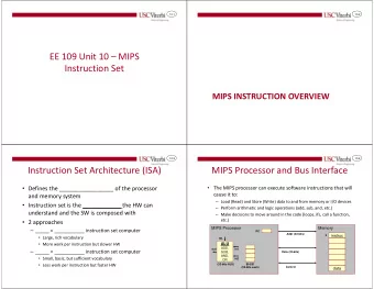
MIPS Architecture w Example: subset of MIPS processor architecture n - PDF document
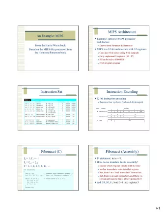
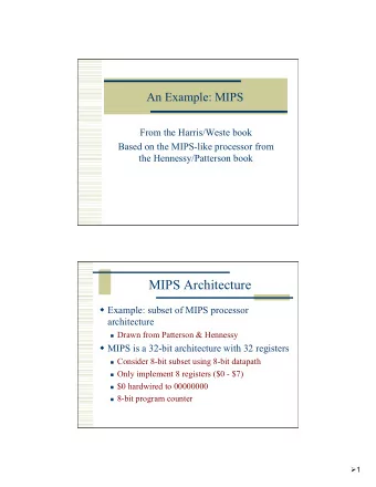
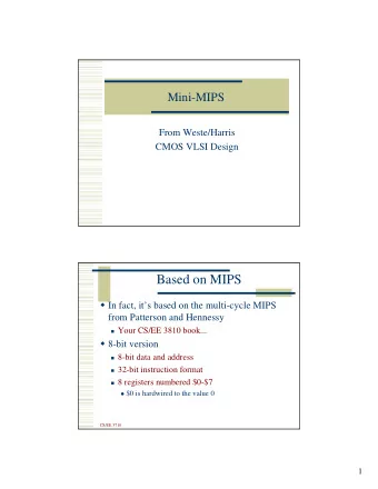
An Example: MIPS From the Harris/Weste book Based on the MIPS-like processor from the Hennessy/Patterson book MIPS Architecture w Example: subset of MIPS processor architecture n Drawn from Patterson & Hennessy w MIPS is a 32-bit
An Example: MIPS From the Harris/Weste book Based on the MIPS-like processor from the Hennessy/Patterson book MIPS Architecture w Example: subset of MIPS processor architecture n Drawn from Patterson & Hennessy w MIPS is a 32-bit architecture with 32 registers n Consider 8-bit subset using 8-bit datapath n Only implement 8 registers ($0 - $7) n $0 hardwired to 00000000 n 8-bit program counter Ø 1
Instruction Set Instruction Set What’s missing from this instruction set? Ø 2
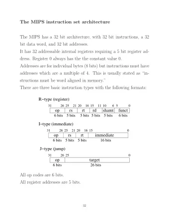
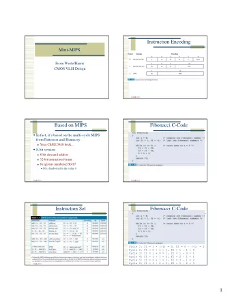
Instruction Set What’s missing from this instruction set? Lots of things! One in particular: Support for subroutine calls… (JAL, STPC, etc.) Instruction Encoding w 32-bit instruction encoding (still 8-bit data) n Requires four cycles to fetch on 8-bit datapath format example encoding 6 5 5 5 5 6 R add $rd, $ra, $rb 0 ra rb rd 0 funct 6 5 5 16 I beq $ra, $rb, imm op ra rb imm 6 26 J j dest op dest Ø 3
Fibonacci (C) f 0 = 1; f -1 = -1 f n = f n-1 + f n-2 f = 0, 1, 1, 2, 3, 5, 8, 13, … Fibonacci (Assembly) w 1 st statement: int n = 8; w How do we translate this to assembly? n Decide which register should hold its value n Load an immediate value into that register n But, there’s no “ load immediate ” instruction… n But, there is an addi instruction, and there’s a convenient register that’s always pinned to 0 w addi $3, $0, 8 ; load 0+8 into register 3 Ø 4
Fibonacci (Assembly) Fibonacci (Binary) w 1 st statement: addi $3, $0, 8 w How do we translate this to machine language? n Hint: use instruction encodings below format example encoding 6 5 5 5 5 6 R add $rd, $ra, $rb 0 ra rb rd 0 funct 6 5 5 16 I beq $ra, $rb, imm op ra rb imm 6 26 J j dest op dest Ø 5
Fibonacci (Binary) w Machine language program Fibonacci (Binary) format example encoding 6 5 5 5 5 6 R add $rd, $ra, $rb 0 ra rb rd 0 funct 6 5 5 16 I beq $ra, $rb, imm op ra rb imm 6 26 J j dest op dest Ø 6
MIPS Microarchitecture w Multicycle microarchitecture from Patterson & Hennessy PCWriteCond PCSource PCEn PCWrite ALUOp Outputs IorD ALUSrcB MemRead ALUSrcA Control MemWrite RegWrite MemtoReg Op RegDst IRWrite[3:0] [5: 0] 0 M 1 u Jump 6 8 Instruction [ 5: 0] address x Shift 2 left 2 Instruction [31:26] PC 0 0 Instruction Read M M [25: 21] register 1 u Address u x Read x Instruction Read A Zero 1 Memory data 1 [20: 16] register 2 1 ALU ALU ALUOut MemData 0 Registers result Instruction M Write Read B [15: 0] u register 0 Instruction data 2 Write [15: 11] x 1 M Instruction 1 Write data register 1 u data 2 x Instruction 0 3 [7: 0] M u x Memory 1 data ALU register control ALUControl Instruction [5: 0] Multicycle Controller Instruction fetch 0 1 2 3 Instruction decode/ MemRead MemRead MemRead MemRead register fetch ALUSrcA = 0 ALUSrcA = 0 ALUSrcA = 0 ALUSrcA = 0 IorD = 0 IorD = 0 IorD = 0 IorD = 0 4 IRWrite3 IRWrite2 IRWrite1 IRWrite0 ALUSrcB = 01 ALUSrcB = 01 ALUSrcB = 01 ALUSrcB = 01 ALUSrcA = 0 ALUOp = 00 ALUOp = 00 ALUOp = 00 ALUOp = 00 ALUSrcB = 11 PCWrite PCWrite PCWrite PCWrite ALUOp = 00 PCSource = 00 PCSource = 00 PCSource = 00 PCSource = 00 ) e ) Q ' (Op = 'J') p y E Reset - t R B = ' O p = (Op = 'LB') or (Op = 'SB ') ( p Memory address O Branch ( Jump computation Execution completion completion 5 9 11 12 ALUSrcA = 1 ALUSrcA = 1 ALUSrcB = 00 ALUSrcA =1 PCWrite ALUSrcB = 10 ALUOp = 01 ALUSrcB = 00 PCSource = 10 ALUOp = 00 PCWriteCond ALUOp= 10 PCSource = 01 (Op = 'S B') (Op = 'L B') Memory Memory access access R-type completion 6 8 10 RegDst = 1 MemRead MemWrite RegWrite IorD = 1 IorD = 1 MemtoReg = 0 Write-back step 7 RegDst=0 RegWrite MemtoReg=1 Ø 7
Logic Design w Start at top level n Hierarchically decompose MIPS into units w Top-level interface memread crystal Clk memwrite oscillator MIPS 8 adr processor 8 external writedata reset memory 8 memdata Verilog Code // top level design includes both mips processor and memory module mips_mem #(parameter WIDTH = 8, REGBITS = 3)(clk, reset); input clk, reset; memread wire memread, memwrite; crystal Clk memwrite oscillator MIPS 8 wire [WIDTH-1:0] adr, writedata; adr processor 8 external writedata reset memory wire [WIDTH-1:0] memdata; 8 memdata // instantiate the mips processor mips #(WIDTH,REGBITS) mips(clk, reset, memdata, memread, memwrite, adr, writedata); // instantiate memory for code and data exmem #(WIDTH) exmem(clk, memwrite, adr, writedata, memdata); endmodule Ø 8
Block Diagram PCWriteCond PCSource PCEn PCWrite ALUOp IorD Outputs ALUSrcB MemRead MemWrite Control ALUSrcA MemtoReg RegWrite IRWrite[3:0] Op RegDst [5: 0] 0 M 1 u Instruction [ 5: 0] 6 8 address Jump x Shift left 2 2 Instruction [31:26] PC 0 0 M Instruction Read u Address [25: 21] register 1 M x u Instruction Read Read A x 1 Memory [20: 16] register 2 data 1 1 Zero MemData 0 ALU ALU ALUOut Instruction Write Registers result [15: 0] M register Read B Instruction u data 2 0 Write Instruction [15: 11] x 1 1 M data register 1 Write u memwrite data 2 x Instruction 0 3 [7: 0] M u x Memory 1 data ALU register control ALUControl memread Instruction [5: 0] controller aluop[1:0] alucontrol op[5:0] zero alusrca alusrcb[1:0] pcen pcsource[1:0] memtoreg regdst iord regwrite irwrite[3:0] funct[5:0] alucontrol[2:0] ph1 ph2 reset datapath adr[7:0] writedata[7:0] memdata[7:0] Top-level // simplified MIPS processor code module mips #(parameter WIDTH = 8, REGBITS = 3) (input clk, reset, input [WIDTH-1:0] memdata, memwrite output memread, memwrite, memread controller output [WIDTH-1:0] adr, writedata); aluop[1:0] alucontrol op[5:0] zero alusrca alusrcb[1:0] pcen pcsource[1:0] memtoreg regdst iord regwrite irwrite[3:0] funct[5:0] alucontrol[2:0] wire [31:0] instr; wire zero, alusrca, memtoreg, iord, pcen; ph1 wire regwrite, regdst; ph2 reset wire [1:0] aluop,pcsource,alusrcb; datapath wire [3:0] irwrite; adr[7:0] writedata[7:0] wire [2:0] alucont; memdata[7:0] controller cont(clk, reset, instr[31:26], zero, memread, memwrite, alusrca, memtoreg, iord, pcen, regwrite, regdst, pcsource, alusrcb, aluop, irwrite); alucontrol ac(aluop, instr[5:0], alucont); datapath #(WIDTH, REGBITS) dp(clk, reset, memdata, alusrca, memtoreg, iord, pcen, regwrite, regdst, pcsource, alusrcb, irwrite, alucont, zero, instr, adr, writedata); endmodule Ø 9
Recommend
More recommend
Explore More Topics
Stay informed with curated content and fresh updates.
