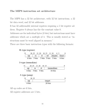
Introduction to the MIPS Architecture January 1416, 2013 1 / 24 - PowerPoint PPT Presentation
Introduction to the MIPS Architecture January 1416, 2013 1 / 24 Unofficial textbook MIPS Assembly Language Programming by Robert Britton A beta version of this book (2003) is available free online 2 / 24 Exercise 1 clarification This is a
Introduction to the MIPS Architecture January 14–16, 2013 1 / 24
Unofficial textbook MIPS Assembly Language Programming by Robert Britton A beta version of this book (2003) is available free online 2 / 24
Exercise 1 clarification This is a question about converting between bases • bit – base-2 (states: 0 and 1) • flash cell – base-4 (states: 0–3) • hex digit – base-16 (states: 0–9, A–F) • Each hex digit represents 4 bits of information: 0xE ⇒ 1110 • It takes two hex digits to represent one byte: 1010 0111 ⇒ 0xA7 3 / 24
Outline Overview of the MIPS architecture What is a computer architecture? Fetch-decode-execute cycle Datapath and control unit Components of the MIPS architecture Memory Other components of the datapath Control unit 4 / 24
What is a computer architecture? One view: The machine language the CPU implements Instruction set architecture (ISA) • Built in data types (integers, floating point numbers) • Fixed set of instructions • Fixed set of on-processor variables (registers) • Interface for reading/writing memory • Mechanisms to do input/output 5 / 24
What is a computer architecture? Another view: How the ISA is implemented Microarchitecture 6 / 24
How a computer executes a program Fetch-decode-execute cycle (FDX) 1. fetch the next instruction from memory 2. decode the instruction 3. execute the instruction Decode determines: • operation to execute • arguments to use • where the result will be stored Execute: • performs the operation • determines next instruction to fetch (by default, next one) 7 / 24
Datapath and control unit Datapath Major hardware components of the FDX cycle • path of instructions and data through the processor • components connected by buses Bus – parallel path for transmitting values • in MIPS, usually 32 bits wide 8 / 24
Datapath and control unit Control unit Controls the components of the datapath • determines how data moves through the datapath • receives condition signals from the components • sends control signals to the components • switches between buses with multiplexers Multiplexer – component for choosing between buses select A MUX out B 9 / 24
Outline Overview of the MIPS architecture What is a computer architecture? Fetch-decode-execute cycle Datapath and control unit Components of the MIPS architecture Memory Other components of the datapath Control unit 10 / 24
Components of the MIPS architecture Major components of the datapath: • program counter (PC) • instruction register (IR) • register file • arithmetic and logic unit (ALU) • memory Control unit http://www.cise.ufl.edu/~mssz/CompOrg/Figure4.3-MIPSarch2.gif 11 / 24
Memory: text segment vs. data segment In MIPS, programs are separated from data in memory Text segment • “instruction memory” • part of memory that stores the program (machine code) • read only Data segment • “data memory” • part of memory that stores data manipulated by program • read/write 12 / 24
Memory: text segment vs. data segment Distinction may or may not be reflected in the hardware: • von Neumann architecture – single, shared memory • Harvard architecture – physically separate memories 13 / 24
Memory addressing in MIPS For reading/writing the data segment Base address plus displacement Memory address computed as base+offset: • base is obtained from a register • offset is given directly as an integer Load word (read word from memory into register): lw $t1,8($t2) ⇒ $t1 := Memory[$t2+8] Store word (write word from register into memory): sw $t1,4($t2) ⇒ Memory[$t2+4] := $t1 We’ll talk about addressing in the text segment later 14 / 24
Program counter (PC) 0x8d0b0000 0x8d0c0004 Program: a sequence of machine instructions 0x016c5020 0xad0a0008 in the text segment 0x21080004 0x2129ffff 0x1d20fff9 Program counter Register that stores the address of the next instruction to fetch • also called the instruction pointer (IP) 15 / 24
Incrementing the PC In MIPS, each instruction is exactly 32-bits long What is the address of the next instruction? PC+4 (Each address refers to one byte, and 32 / 8 = 4) 16 / 24
Instruction register (IR) Instruction register Register that holds the instruction currently being decoded Note condition signals from the IR to the control unit! 17 / 24
Register file Register : component that stores a 32-bit value MIPS register file contains 32 registers 18 / 24
Register names and conventions Number Name Usage Preserved? constant 0x00000000 N/A $0 $zero ✗ assembler temporary $1 $at ✗ $2 – $3 $v0 – $v1 function return values ✗ $4 – $7 $a0 – $a3 function arguments ✗ $8 – $15 $t0 – $t7 temporaries ✓ $16 – $23 $s0 – $s7 saved temporaries ✗ $24 – $25 $t8 – $t9 more temporaries $26 – $27 $k0 – $k1 reserved for OS kernel N/A ✓ global pointer $28 $gp ✓ stack pointer $29 $sp ✓ frame pointer $30 $fp ✓ return address $31 $ra 19 / 24
Arithmetic and logic unit (ALU) Implements binary arithmetic and logic operations Inputs : Outputs : • operands – 2 × 32-bit • result – 1 × 64-bit • operation – control signal (usually just use 32 bits of this) • status – condition signals 20 / 24
Control unit Controls components of datapath to implement FDX cycle • Inputs : condition signals • Outputs : control signals Implemented as a finite state machine 21 / 24
MIPS data path with control signals http://fourier.eng.hmc.edu/e85/lectures/figures/MIPS_datapath_control.gif 22 / 24
Control unit Condition signals • from IR – decode operation, arguments, result location • from ALU – overflow, divide-by-zero, . . . Control signals • to multiplexors – buses to select • to each register – load new value • to ALU – operation to perform • to all – clock signal 23 / 24
Clock signal Each component is implemented as an electrical circuit • when inputs change, outputs change – not instantaneous! • clock signal ensures we don’t use outputs until ready Clock generator produces the clock signal 1 0 ↑ ↑ ↑ ↑ • synchronizes the components in the data path • the faster the clock, the faster the program executes • clock rate is limited by the slowest component! 24 / 24
Recommend
More recommend
Explore More Topics
Stay informed with curated content and fresh updates.
