Instruction Encoding Mini-MIPS From Weste/Harris CMOS VLSI Design - PDF document
Instruction Encoding Mini-MIPS From Weste/Harris CMOS VLSI Design CS/EE 3710 Based on MIPS Fibonacci C-Code In fact, its based on the multi-cycle MIPS from Patterson and Hennessy Your CS/EE 3810 book... 8-bit version 8-bit
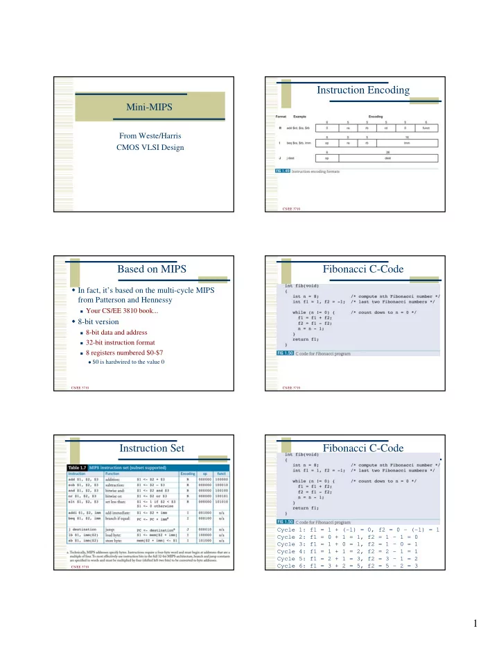
Instruction Encoding Mini-MIPS From Weste/Harris CMOS VLSI Design CS/EE 3710 Based on MIPS Fibonacci C-Code � In fact, it’s based on the multi-cycle MIPS from Patterson and Hennessy � Your CS/EE 3810 book... � 8-bit version � 8-bit data and address � 32-bit instruction format � 8 registers numbered $0-$7 � $0 is hardwired to the value 0 CS/EE 3710 CS/EE 3710 Instruction Set Fibonacci C-Code Cycle 1: f1 = 1 + (-1) = 0, f2 = 0 – (-1) = 1 Cycle 2: f1 = 0 + 1 = 1, f2 = 1 – 1 = 0 Cycle 3: f1 = 1 + 0 = 1, f2 = 1 – 0 = 1 Cycle 4: f1 = 1 + 1 = 2, f2 = 2 – 1 = 1 Cycle 5: f1 = 2 + 1 = 3, f2 = 3 – 1 = 2 Cycle 6: f1 = 3 + 2 = 5, f2 = 5 – 2 = 3 CS/EE 3710 CS/EE 3710 1
Fibonacci Assembly Code Architecture Compute 8 th Fibonacci number (8’d13 or 8’h0D) Store that number in memory location 255 CS/EE 3710 CS/EE 3710 Fibonacci Machine Code Another View 4 101000 Machine Code Assembly Code CS/EE 3710 CS/EE 3710 Architecture Control FSM CS/EE 3710 CS/EE 3710 2
Connection to External Memory Exmem.v module exmem #(parameter WIDTH = 8, RAM_ADDR_BITS = 8) (input clk, en, input memwrite, input [RAM_ADDR_BITS-1:0] adr, input [WIDTH-1:0] writedata, output reg [WIDTH-1:0] memdata); reg [WIDTH-1:0] mips_ram [(2**RAM_ADDR_BITS)-1:0]; initial $readmemb("fib.dat", mips_ram); This is synthesized to a Block RAM on the always @(posedge clk) if (en) begin Spartan3e FPGA if (memwrite) mips_ram[adr] <= writedata; memdata <= mips_ram[adr]; end Note clock! endmodule CS/EE 3710 CS/EE 3710 External Memory from Book Block RAM // external memory accessed by MIPS assign word = RAM[adr>>2]; module exmemory #(parameter WIDTH = 8) always @(*) (input clk, case (adr[1:0]) input memwrite, 2'b00: memdata <= word[7:0]; input [WIDTH-1:0] adr, writedata, 2'b01: memdata <= word[15:8]; output reg [WIDTH-1:0] memdata); 2'b10: memdata <= word[23:16]; 2'b11: memdata <= word[31:24]; reg [31:0] RAM [(1<<WIDTH-2)-1:0]; endcase wire [31:0] word; endmodule Byte-wide Block RAM is // Initialize memory with program Notes: initial $readmemh("memfile.dat",RAM); really 9-bits – parity bit... • Endianess is fixed here // read and write bytes from 32-bit word • Writes are on posedge clk always @(posedge clk) if(memwrite) • Reads are asynchronous case (adr[1:0]) • This is a 32-bit wide RAM 2'b00: RAM[adr>>2][7:0] <= writedata; 2'b01: RAM[adr>>2][15:8] <= writedata; • With 64 locations 2'b10: RAM[adr>>2][23:16] <= writedata; • But with an 8-bit interface... 2'b11: RAM[adr>>2][31:24] <= writedata; endcase (Actually dual ported too!) CS/EE 3710 CS/EE 3710 Exmem.v Our Block Ram � Read-first or Write-first? module exmem #(parameter WIDTH = 8, RAM_ADDR_BITS = 8) (input clk, en, input memwrite, always @(posedge clk) input [RAM_ADDR_BITS-1:0] adr, if (en) begin input [WIDTH-1:0] writedata, output reg [WIDTH-1:0] memdata); if (memwrite) reg [WIDTH-1:0] mips_ram [(2**RAM_ADDR_BITS)-1:0]; mips_ram[adr] <= writedata; initial $readmemb("fib.dat", mips_ram); memdata <= mips_ram[adr]; •This is synthesized to always @(posedge clk) a Block RAM on the end if (en) begin Spartan3e FPGA if (memwrite) • It’s 8-bits wide mips_ram[adr] <= writedata; memdata <= mips_ram[adr]; • With 256 locations end • Both writes and reads are clocked endmodule CS/EE 3710 CS/EE 3710 3
Read_First Template Write_First Waveforms CS/EE 3710 CS/EE 3710 Write_First Template Block RAM Organization Block RAM is Single or Dual ported Each block is 18k bits... CS/EE 3710 CS/EE 3710 Read_First waveforms Recall – Overall System Clk Clock Clk CS/EE 3710 CS/EE 3710 4
Recall – Overall System Controller Clk Clock State Codes Clk Useful constants to compare against So, what are the implications of using a RAM that has both clocked reads and writes instead of clocked writes and async reads? (we’ll come back to this question...) State Register CS/EE 3710 CS/EE 3710 mips Block Diagram Control FSM CS/EE 3710 CS/EE 3710 mips.v Next State Logic // simplified MIPS processor module mips #(parameter WIDTH = 8, REGBITS = 3) (input clk, reset, input [WIDTH-1:0] memdata, output memread, memwrite, output [WIDTH-1:0] adr, writedata); wire [31:0] instr; wire zero, alusrca, memtoreg, iord, pcen, regwrite, regdst; wire [1:0] aluop,pcsource,alusrcb; wire [3:0] irwrite; wire [2:0] alucont; controller cont(clk, reset, instr[31:26], zero, memread, memwrite, alusrca, memtoreg, iord, pcen, regwrite, regdst, pcsource, alusrcb, aluop, irwrite); alucontrol ac(aluop, instr[5:0], alucont); datapath #(WIDTH, REGBITS) dp(clk, reset, memdata, alusrca, memtoreg, iord, pcen, regwrite, regdst, pcsource, alusrcb, irwrite, alucont, zero, instr, adr, writedata); endmodule CS/EE 3710 CS/EE 3710 5
Output Logic ALU Very common way to deal with default values in combinational Invert b if subtract... Always blocks add is a + b sub is a + ~b +1 subtract on slt then check if answer is negative Continued for the other states... CS/EE 3710 CS/EE 3710 Output Logic zerodetect Two places to update the PC pcwrite on jump pcwritecond on BEQ Why AND these two? CS/EE 3710 CS/EE 3710 ALU Control Register File What is this synthesized into? CS/EE 3710 CS/EE 3710 6
Synthesis Report Datapath Fairly complex... Not really, but it does have lots of registers instantiated directly It also instantiates muxes... Instruction Register CS/EE 3710 CS/EE 3710 Synthesis Report Datapath continued RF and ALU Flops and muxes... CS/EE 3710 CS/EE 3710 Synthesis Report Flops and MUXes Two register files? Why? CS/EE 3710 CS/EE 3710 7
Back to the Memory Question Instruction Fetch � What are the implications of using RAM that is clocked on both write and read? � Book version was async read � So, let’s look at the sequence of events that happen to read the instruction � Four steps – read four bytes and put them in four slots in the 32-bit instruction register (IR) • Memread, irwrite, addr, etc are set up just after clk edge • Data comes back sometime after that (async) • Data is captured in ir0 – ir3 on the next rising clk edge • How does this change if reads are clocked? CS/EE 3710 CS/EE 3710 Instruction Fetch mips + exmem mips is expecting async reads exmem has clocked reads One of those rare cases where using both edges of the clock is useful! CS/EE 3710 CS/EE 3710 Instruction Fetch Memory Mapped I/O � Break memory space into pieces (ranges) � For some of those pieces: regular memory � For some of those pieces: I/O � That is, reading from an address in that range results in getting data from an I/O device � Writing to an address in that range results in data going to an I/O device CS/EE 3710 CS/EE 3710 8
Mini-MIPS Memory Map Lab2 in a Nutshell FF 8-bit � Understand and simulate mips/exmem 1111 1111 I/O addresses Switches/LEDs � Add ADDI instruction 1100 0000 C0 256 bytes � Fibonacci program – correct if 8’0d is written to BF total! 1011 1111 memory location 255 Code/Data � Augment the system 1000 0000 80 Top two address � Add memory mapped I/O to switches/LEDs bits define regions 0111 1111 7F Code/Data � Write new Fibonacci program 0100 0000 40 � Simulate in ISE 0011 1111 3F � Demonstrate on your board Code/Data 64 bytes 0000 0000 00 CS/EE 3710 CS/EE 3710 Enabled Devices My Initial Testbench... Only write to that device (i.e. enable it) if you’re in the appropriate memory range. Check top two address bits! CS/EE 3710 CS/EE 3710 MUXes for Return Data My Initial Results Use MUX to decide if data is coming from memory or from I/O Check address bits! CS/EE 3710 CS/EE 3710 9
Recommend
More recommend
Explore More Topics
Stay informed with curated content and fresh updates.
