Logic Minimization M. Sachdev, Dept. of Electrical & Computer - PDF document
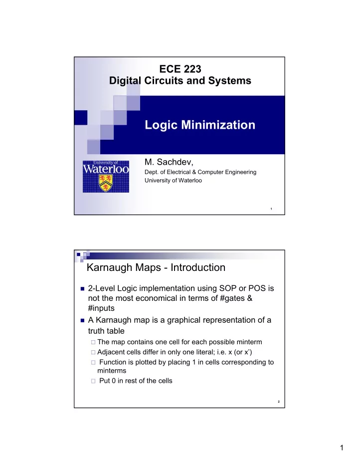
ECE 223 Digital Circuits and Systems Logic Minimization M. Sachdev, Dept. of Electrical & Computer Engineering University of Waterloo 1 Karnaugh Maps - Introduction 2-Level Logic implementation using SOP or POS is not the most
ECE 223 Digital Circuits and Systems Logic Minimization M. Sachdev, Dept. of Electrical & Computer Engineering University of Waterloo 1 Karnaugh Maps - Introduction � 2-Level Logic implementation using SOP or POS is not the most economical in terms of #gates & #inputs � A Karnaugh map is a graphical representation of a truth table � The map contains one cell for each possible minterm � Adjacent cells differ in only one literal; i.e. x (or x’) � Function is plotted by placing 1 in cells corresponding to minterms � Put 0 in rest of the cells 2 1
K Map with 2 Variables � F =f(x,y) y x y F x 0 1 0 0 m0 0 m0 m1 0 1 m1 1 0 m2 1 m2 m3 1 1 m3 y � Example, F1 = x’y x 0 1 0 1 3 K Map with 3 Variables 3 Variable, F = f(x,y,z); � yz Given F2 = ∑ (2,3,4,5) � x 00 01 11 10 Represent it on the K map � minimize the function � 0 m0 m1 m3 m2 yz 1 m4 m5 m7 m6 x 00 01 11 10 0 yz x 00 01 11 10 1 0 x’y’z’ ’x’y’z x’yz x’yz’ 1 xy’z’ xy’z xyz xyz’ 4 2
K Map with 3 Variables 3 Variable, F = f(x,y,z); � Given F3 = ∑ (3,4,6,7) � Minimize the function using K map � Function minimization Find maximum size groups that cover all 1s in the map � (Comment – a group should not be a subset of other group) 4 cell group � 2 literals can be removed 2 cell group � 1 literal can be removed Guidelines for logic synthesis (SOP) � Fewer groups � fewer AND gates, and fewer inputs to the � OR gate Fewer literals (larger group) � fewer inputs to an AND gate � Synthesis Objective: Fewest # of gates and # of inputs � 5 K Map with 4 Variables yz wx 00 01 11 10 4 Variable, F = f(w,x,y,z) � 00 m0 m1 m3 m2 Given, F4 = ∑ (3,4,5,7,9,13,14,15) � 01 m4 m5 m7 m6 represent it on the map � Minimize the logic � 11 m12 m13 m15 m14 10 m8 m9 m11 m10 Clues � Make all possible groups � yz Do we need “the group of 4”? wx 00 01 11 10 � 00 0 0 1 0 F4 = w’xy’ +wxy +w’yz +wy’z 01 0 1 1 0 11 1 1 1 1 10 0 1 0 0 6 3
Implicants & Prime Implicants, … Implicant: A group of one or more k map cell � Prime implicant: an implicant that is not a subset of � another implicant Essential Prime Implicant: a prime implicant that covers � at least one cell not covered by another prime implicant Example, F5 (w,x,y,z) = ∑ (0,1,2,5,6,7,9,13,14) � yz yz wx 00 01 11 10 wx 00 01 11 10 00 1 1 0 1 00 1 1 0 1 01 0 1 1 1 01 0 1 1 1 11 0 1 0 1 11 0 1 0 1 10 0 1 0 0 10 0 1 0 0 7 Product of Sum Expression Let F be the function � F’ = ∑ (all minterms not in F) � F = π (all minterms not in F)’ (de Morgan’s theorem) � Therefore, one cam obtain POS expression by � Group all 0s on K map 1. Use de Morgan’s theorem to obtain POS expression 2. F6 = x’z’ +x’y’ + w’y’z (SOP) = (w’ +x’)(y’ +z’)(x’ +z) (POS) One is often simpler than the other � Check both � yz yz wx 00 01 11 10 wx 00 01 11 10 00 1 1 0 1 00 1 1 0 1 01 0 1 0 0 01 0 1 0 0 11 0 0 0 0 11 0 0 0 0 10 1 1 0 1 10 1 1 0 1 8 4
Plotting Product of Sum Expression Given, F7 = (w +x)(x +y’ +z)(y +z) � yz wx 00 01 11 10 F7’ = [(w +x)(x +y’ +z)(y +z)]’ = (w +x)’ +(x +y’ +z)’ +(y +z)’ 00 0 0 0 0 = w’x’ +x’yz’ +y’z’ 01 0 1 1 1 F7’ is plotted by putting 0s in � appropriate cells 11 0 1 1 1 Can F7’ be simplified further? � 10 0 1 1 0 F7’ = w’x’ +x’z’ +y’z’ F7 = (w +x)(x +z)(y +z) 9 Don’t care Conditions Some time, not all values of a function are defined � Some inputs conditions will never occur � We don’t care what the output is for that input condition � In these cases, we can choose the output to be wither � 0 or 1, whichever simplifies the circuit Example – A circuit to produce output 1 if a BCD digit � is multiple of 3 BCD – Four inputs (wxyz) 0 (0000) � 9 (1001) � Values of wxyz 10 (1010) � 15 (1111) don’t care � The function F8 = ∑ (3,6,9) +d(10,11,12,13,14,15) � 10 5
Don’t Care - Plotting Don’t care are plotted as X in the K map � SOP expression � Treat X as 1 if it allows a larger group � POS expression � Treat x as 0 if it allows a larger group � F8_1 = wz +xyz’ +x’yz (SOP) � F8’_2 = xz +w’y’ +x’z’ {F’ = ∑ (all minterms not in F)} F8_2 = (x’ +z’)(w +y)(x +z) de Morgan’s theorem Is F8_1 = F8_2?? yz yz wx 00 01 11 10 wx 00 01 11 10 00 0 0 1 0 00 0 0 1 0 01 0 0 0 1 01 0 0 0 1 11 X X X X 11 X X X X 10 0 1 X X 10 0 1 X X 11 Simplest 2-Level Expression Example, F(w,x,y,z) = ∑ (0,1,2,5,6,7,9,14) +d(13) � Determine essential and prime implicants � yz yz wx 00 01 11 10 wx 00 01 11 10 00 1 1 0 1 00 1 1 0 1 01 0 1 1 1 01 0 1 1 1 11 0 X 0 1 11 0 X 0 1 10 0 1 0 0 10 0 1 0 0 Essential prime implicants Prime implicants 12 6
Simplest 2-Level Expression Example, F(w,x,y,z) = ∑ (0,1,2,5,6,7,9,14) +d(13) � Determine essential and prime implicants � 0 1 2 5 6 7 9 14 y’z (1,5,9,13) √ √ √ ۞ xyz’ (6,14) √ √ ۞ w’x’y’ (0,1) √ √ A w’x’z’ (0,2) √ √ B w’xz (5,7) √ √ C w’xy (6,7) √ √ D w’yz’ (2,6) √ √ E All minterms must be covered � i.e., essential prime implicants must be included � Different choices for prime implicants � B +C; or B +D; or A +C +E; or A +D +E 13 Tabulation (Quine-McCluskey) Method The map method of simplification is convenient if # of � variables ≤ 4 Tabulation method is preferred for function with large # of variables � For F(w,x,y,z) consider adjacent minterms � let a = m4 +m5 = w’xy’z’ + w’xy’z = w’xy’ or = 0100 + 0101 = 010- Similarly, b =m12 +m13 = wxy’z’ + wxy’z = wxy’ = 110- Let c = a +b = m4 +m5 +m12 +m13 � w’xy’ +wxy’ = xy’ = -10- Adjacent terms differ by a single bit in their representation � Tabulation method consists of grouping of minterms and � systematically checking for single bit differences 14 7
Tabulation (Quine-McCluskey) Method Example, F(w,x,y,z) = ∑ (0,3,4,6,7,8,10,11,15) +d(5,9) � Place minterms in different Sections according to # of 1’s in their � binary representation Each member of each Section is compared with each member of � Sections below; all reduction are recorded in next column Mark terms that combine � All unmarked terms are prime implicants � 15 Tabulation Method - Example Example � 16 8
NAND & NOR Implementation In digital logic families NAND & NOR implementations � are cheaper compared to AND & OR implementations Hence, NAND & NOR are preferred � NAND and NOR are universal gates � Can mimic any logic gate � Example, NAND gate can implement: � NOT � short inputs AND � {(xy)’}’ OR � (x’y’)’ = x +y Similarly for NOR gate, one can show its universality � 17 NAND – 2-level Implementation Can implement any arbitrary logic � Example, F = AB + CD 18 9
NAND – 2-level Implementation Given, F9 (x,y,z) = ∑ (1,2,3,4,5,7) � Minimize the function, and implement it with NAND gates 19 NAND – 2-level Implementation Procedure Simplify the function and express it in SOP form 1. Draw a NAND gate for each product term 2. Draw a single gate using AND-invert or invert-OR 3. symbol for the sum term A term with single literal, complement if needed 4. Multi-level NAND Circuits � Convert all AND gates to NAND gates 1. Convert all OR gates to NAND gates with invert-OR 2. symbols Balance all bubbles, insert an inverter if needed 3. 20 10
NOR – Implementation NOR gate is a dual of NAND � Same rules and procedures � Example, F = (A +B)(C +D)E 21 Wired Logic Two logic gate outputs are not shorted together � May create logical conflicts � Logic is not defined � In some technologies, it is possible to short O/Ps � of some logic gates (wired logic) F1 = (AB)’(CD)’ = (AB + CD)’ (wired AND) F2 = (A +B)’ + (C +D)’ = [A +B)(C +D)]’ (wired OR) 22 11
Exclusive-OR Function XOR gate is expensive to implement in silicon � XOR = xy’ +x’y XNOR = (xy’ +x’y)’ = xy +x’y’ But they are useful in � Parity checking � Arithmetic circuits (adders, subtractors) � x y XOR XNOR 0 0 0 1 0 1 1 0 1 0 1 0 1 1 0 1 23 Exclusive-OR Function XOR gate properties � Commutative � Associative � Odd and Even Functions � 24 12
Exclusive-OR Function 4 Variable XOR � 25 Parity Generation and Checking Parity checking is useful for detecting and � correcting errors when transmitting binary data We can always append a parity bit to the end of the � data bits (e.g. 32) so that the number of 1s in the packet is always even or odd If we lose a bit in transmission, we can use the � parity bit to tell us there has been a problem 26 13
Book Sections – Logic Minimization � Material is covered in Sections 3.1 – 3.8 27 14
Recommend
More recommend
Explore More Topics
Stay informed with curated content and fresh updates.
