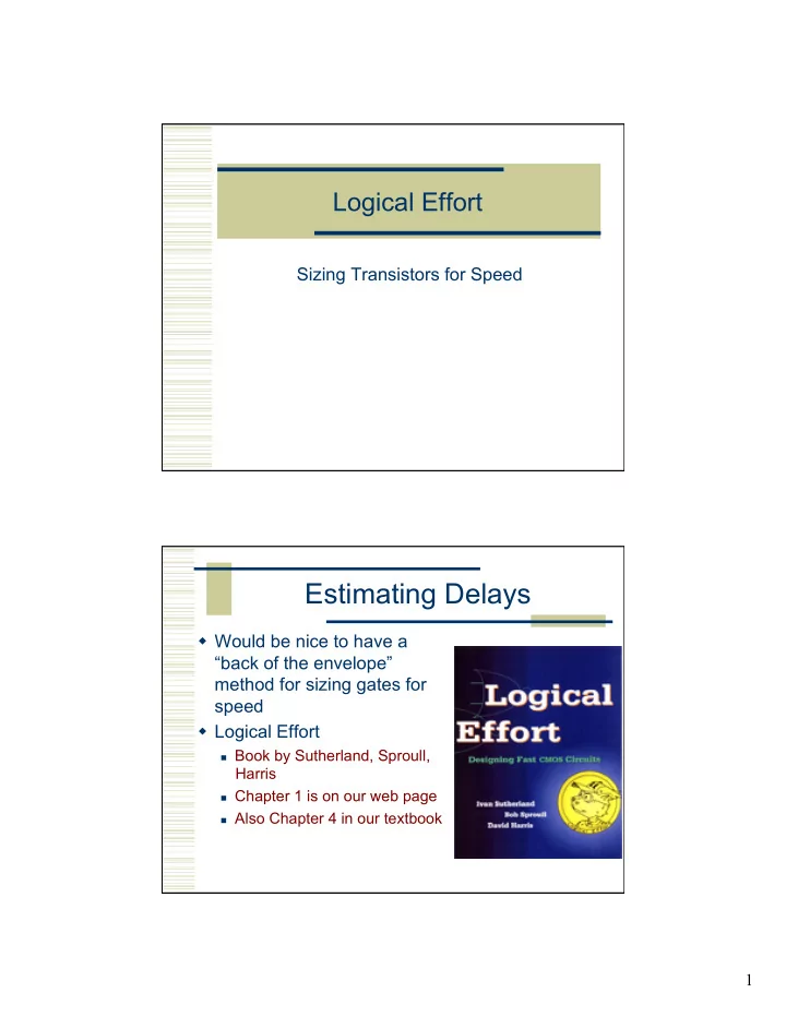
Estimating Delays Would be nice to have a back of the envelope - PDF document
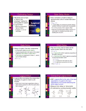
Logical Effort Sizing Transistors for Speed Estimating Delays Would be nice to have a back of the envelope method for sizing gates for speed Logical Effort Book by Sutherland, Sproull, Harris Chapter 1 is on our web page
Logical Effort Sizing Transistors for Speed Estimating Delays Would be nice to have a “back of the envelope” method for sizing gates for speed Logical Effort Book by Sutherland, Sproull, Harris Chapter 1 is on our web page Also Chapter 4 in our textbook 1
Gate Delay Model First, normalize a model of delay to dimensionless units to isolate fabrication effects d abs = d τ τ is the delay of a minimum inverter driving another minimum inverter with no parasitics In a 0.6u process, this is approx 40ps Now we can think about delay in terms of d and scale it to whatever process we’re using Gate Delay Delay of a gate d has two components A fixed part called parasitic delay p A part proportional to the load on the output called the effort delay or stage effort f Total delay is measured in units of τ , and is sum of these delays d = f + p 2
Effort Delay The effort delay (due to load) can be further broken down into two terms: f = g * h g = logical effort which captures properties of the gate’s structure h = electrical effort which captures properties of load and transistor sizes h = C out /C in C out is capacitance that loads the output C in is capacitance presented at the input So, d = gh + p Logical Effort Logical effort normalizes the output drive capability of a gate to match a unit inverter How much more input capacitance does a gate need to present to offer the same drive as an inverter? g = 5/3 g = 1 g = 4/3 3
Computing Logical Effort DEF: Logical effort is the ratio of the input capacitance of a gate to the input capacitance of an inverter delivering the same output current . Measure from delay vs. fanout plots Or estimate by counting transistor widths Logical Effort of Other Gates Logical effort of common gates assuming that P/N size ratio is 2 Number of inputs 4
Electrical Effort Value of logical effort g is independent of transistor size It’s related to the ratios and the topology Electrical effort h captures the drive capability of the transistors via sizing Electrical effort h = C out /C in Note that as transistor sizes for a gate increase, h decreases because C in goes up Parasitic Delay Parasitic delay p is caused by the internal capacitance of the gate It’s constant and independent of transistor size As you increase the transistor size, you also increase the cap of the gate/source/drain areas which keeps it constant For our purposes, normalize p inv to 1 N-input NAND = n*p inv N-input NOR = n*p inv N-way mux = 2n*p inv XOR = 4* p inv 5
Plots of Gate Delay Delay Estimation Remember, τ in Our process ~ 40ps ~200ps ~240ps 6
Delay Estimation Remember, τ in Our process ~ 40ps ~200ps τ in 180nm = ~ 12ps FO4 Inverter delay = 60ps FO4 NAND delay = 72ps ~240ps Example: Ring Oscillator Estimate the frequency of an N-stage ring oscillator Logical Effort: g = Electrical Effort: h = Parasitic Delay: p = Stage Delay: d = Period of osc = 7
Example: Ring Oscillator Estimate the frequency of an N-stage ring oscillator Logical Effort: g = 1 Electrical Effort: h = 1 Parasitic Delay: p = 1 Stage Delay: d = 2 so d abs = 80ps Period: 2*N*d abs = 4.96ns, Freq = ~200MHz For N = 31 Example: FO4 Inverter Estimate the delay of a fanout-of-4 (FO4) inverter Logical Effort: g = Electrical Effort: h = Parasitic Delay: p = Stage Delay: d = 8
Example: FO4 Inverter Estimate the delay of a fanout-of-4 (FO4) inverter The FO4 delay is about 200 ps in 0.6 µ m process 60 ps in a 180 nm process Logical Effort: g = 1 f/3 ns in an f µ m process Electrical Effort: h = 4 Parasitic Delay: p = 1 Stage Delay: d = gh + p = 5 Delay Estimation If Cin = x, Cout = 10x, thus h = 10 g = 9/3 = 3 d = gh + p = 3*10 + 4*1 = 34 (1360 ps) 9
Multi Stage Delay Off-Path Load Ctotal Cuseful 10
Summary – multistage networks Logical effort generalizes to multistage networks Path Logical Effort Path Electrical Effort Path Effort Can we write F = GH? Branching Effort Remember branching effort Accounts for branching between stages in path Note: Now we compute the path effort F = GBH 11
Multistage Delays Path Effort Delay Path Parasitic Delay Path Delay Designing Fast Circuits Delay is smallest when each stage bears same effort Thus minimum delay of N stage path is This is a key result of logical effort Find fastest possible delay Doesn’t require calculating gate sizes 12
Minimizing Path Delay Choosing Transistor Sizes 13
Example 0 1 2 minD=N*F 1/N + P = 3*(1.3333) + 6 = 10 Example, continued f(min) = gi * bi * hi 14
Transistor Sizes for Example Another Example, Larger Load 15
8C Load Example Cont. Example 1.6 from Chap 1 0 1 2 16
Example 1.6 Continued f(min) = gi * bi * hi Example: 3-stage path Select gate sizes x and y for least delay from A to B 17
Example: 3-stage path Logical Effort G = Electrical Effort H = Branching Effort B = Path Effort F = Best Stage Effort Parasitic Delay P = Delay D = Example: 3-stage path Logical Effort G = (4/3)*(5/3)*(5/3) = 100/27 Electrical Effort H = 45/8 Branching Effort B = 3 * 2 = 6 Path Effort F = GBH = 125 Best Stage Effort Parasitic Delay P = 2 + 3 + 2 = 7 Delay D = 3*5 + 7 = 22 = 4.4 FO4 18
Example: 3-stage path Work backward for sizes y = x = Example: 3-stage path f(min) = gi * bi * hi Work backward for sizes y = 45 * (5/3) / 5 = 15 (g i *b i *C out )/f min = C in x = (15*2) * (5/3) / 5 = 10 8 10 15 1:1 ratio 2:3 ratio 4:1 ratio 19
Example 1.7 from Chap 1 (g i *b i *C out )/f min =C in Note: Don’t care about parasitics for gate sizing, only if you want to know absolute delay… Misc. Comments Note that you never size the first gate This gate is assumed to be fixed If you were allowed to size it, the algorithm would try to make it as large as possible This is an estimation algorithm Authors claim that sizing a gate by 1.5x too big or small still results in a path delay within 15% of minimum 20
Sensitivity Analysis How sensitive is delay to using exactly the best number of stages? 2.4 < ρ < 6 gives delay within 15% of optimal We can be sloppy! I like ρ = 4 Evaluating Different Options 21
Option #1 Option #2 What if we consider gate area and power? What about a 4-input NOR? 22
How many stages? Consider three alternatives for driving a load 25 times the input capacitance One inverter Three inverters in series Five inverters in series They all do the job, but which one is fastest? How many stages? In all cases: G = 1, B = 1, and H = 25 Path delay is N(25) 1/N + N P inv N = 1, D = 26 units N = 3, D = 11.8 units N = 5, D = 14.5 units Since N=3 is best, each stage will bear an effort of (25) 1/3 = 2.9 So, each stage is ~3x larger than the last In general, the best stage effort is between 3 and 4 (not e as often stated) The e value doesn’t use parasitics… 23
Choosing the Best # of Stages You can solve the delay equations to determine the number of stages N that will achieve the minimum delay Approximate by Log 4 F Example String of inverters driving an off-chip load Pad cap and load = 40pf Equivalent to 20,000 microns of gate cap Assume first inverter in chain has 7.2u of input cap How many stages in inv chain? H = 20,000/7.2 = 2777 From the table, 6 stages is best Stage effort = f = (2777) 1/6 = 3.75 Path delay D = 6*3.75 +6*Pinv = 28.5 D = 1.14ns if τ = 40ps 24
Other N’s? N=2: f=(2777) 1/2 = 52.7 delay = 2(52.7) +2 = 158.1 = 6.324ns N=3: f=(2777) 1/3 = 14 delay = 3(14) +3 = 45 = 1.8ns N=4: f=(2777) 1/4 = 7.26 delay = 4(7.26) + 4 = 33.04 = 1.32ns N=5: f=(2777) 1/5 = 4.88 delay = 5(4.88) +5 = 29.4 = 1.18ns N=6: delay = 1.14ns N=7: f=(2777) 1/7 = 3.105 delay = 7(3.105) +7 = 28.7 = 1.15ns Summary Compute path effort F = GBH Use table, or estimate N = log 4 F to decide on number of stages Estimate minimum possible delay D = NF 1/N + Σ p i Add or remove stages in your logic to get close to N Compute effort at each stage f min = F 1/N Starting at output, work backwards to compute transistor sizes C in = (g i * b i * C out )/f min 25
Limits of Logical Effort Chicken and egg problem Need path to compute G But don’t know number of stages without G Simplistic delay model Neglects input rise time effects Interconnect Iteration required in designs with wire Maximum speed only Not minimum area/power for constrained delay Summary Logical effort is useful for thinking of delay in circuits Numeric logical effort characterizes gates NANDs are faster than NORs in CMOS Paths are fastest when effort delays are ~4 Path delay is weakly sensitive to stages, sizes But using fewer stages doesn’t mean faster paths Delay of path is about log 4 F FO4 inverter delays Inverters and NAND2 best for driving large caps Provides language for discussing fast circuits But requires practice to master 26
Recommend
More recommend
Explore More Topics
Stay informed with curated content and fresh updates.










![2 ) 1 2 ( r r )= Ne ( 1 + r ] ) E ( [ 1 e 2 0 r r LHC BBC](https://c.sambuz.com/778155/2-s.webp)