Estimating Delays Gate Delay Model Would be nice to have First, - PDF document
Estimating Delays Gate Delay Model Would be nice to have First, normalize a model of delay to a back of the dimensionless units to isolate fabrication envelope method for effects d abs = d sizing gates for speed is
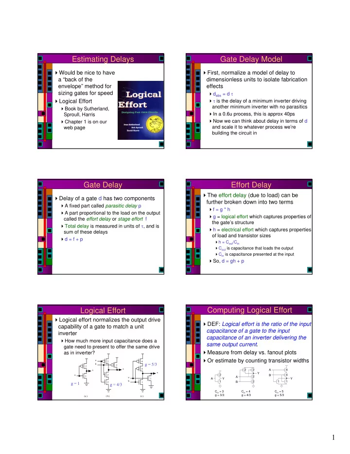
Estimating Delays Gate Delay Model � Would be nice to have � First, normalize a model of delay to a “back of the dimensionless units to isolate fabrication envelope” method for effects � d abs = d τ sizing gates for speed � τ is the delay of a minimum inverter driving � Logical Effort another minimum inverter with no parasitics � Book by Sutherland, � In a 0.6u process, this is approx 40ps Sproull, Harris � Now we can think about delay in terms of d � Chapter 1 is on our and scale it to whatever process we’re web page building the circuit in Gate Delay Effort Delay � The effort delay (due to load) can be � Delay of a gate d has two components further broken down into two terms � A fixed part called parasitic delay p � f = g * h � A part proportional to the load on the output � g = logical effort which captures properties of called the effort delay or stage effort f the gate’s structure � Total delay is measured in units of τ , and is � h = electrical effort which captures properties sum of these delays of load and transistor sizes � d = f + p � h = C out /C in � C out is capacitance that loads the output � C in is capacitance presented at the input � So, d = gh + p Computing Logical Effort Logical Effort � Logical effort normalizes the output drive � DEF: Logical effort is the ratio of the input capability of a gate to match a unit capacitance of a gate to the input inverter capacitance of an inverter delivering the � How much more input capacitance does a same output current . gate need to present to offer the same drive � Measure from delay vs. fanout plots as in inverter? � Or estimate by counting transistor widths a 2 4 g = 5/3 b 2 2 x 4 x 2 2 A 4 x Y a 2 2 4 B 1 2 A a 1 A Y Y b 1 2 1 1 g = 1 2 1 B g = 4/3 C in = 3 C in = 4 C in = 5 g = 3/3 g = 4/3 g = 5/3 (a ) (b ) (c) 1
Logical Effort of Other Gates Electrical Effort � Logical effort of common gates assuming � Value of logical effort g is independent of that P/N size ratio is 2 transistor size � It’s related to the ratios and the topology Number of inputs � Electrical effort h captures the drive Gate Type 1 2 3 4 5 n capability of the transistors via sizing Inverter 1 � Electrical effort h = C out /C in NAND 4/3 5/3 6/3 7/3 (n+2)/3 NOR 5/3 7/3 9/3 11/3 (2n+1)/3 � Note that as transistor sizes for a gate MUX 2 2 2 2 2 increase, h decreases because C in goes up XOR 4 12 32 Parasitic Delay Plots of Gate Delay 6 � Parasitic delay p is caused by the internal Two-input NAND : g = , p = 2 capacitance of the gate 4 5 3 � It’s constant and independent of transistor size 4 Inverter: g = 1, p = 1 � As you increase the transistor size, you also 3 increase the cap of the gate/source/drain Effort delay areas which keeps it constant 2 � For our purposes, normalize p inv to 1 � N-input NAND = n*p inv 1 � N-input NOR = n*p inv Parasitic delay � N-way mux = 2n*p inv 0 0 1 2 3 4 5 � XOR = 4* p inv Electrical effort: h Delay Estimation Delay Estimation Remember, τ in Remember, τ in Our process ~ 40ps Our process ~ 40ps ~200ps ~200ps τ in 180nm = ~ 12ps FO4 Inverter delay = 60ps FO4 NAND delay = 72ps ~240ps ~240ps 2
Example: Ring Oscillator Example: Ring Oscillator � Estimate the frequency of an N-stage ring � Estimate the frequency of an N-stage ring oscillator oscillator Logical Effort: g = Logical Effort: g = 1 Electrical Effort: h = Electrical Effort: h = 1 Parasitic Delay: p = Parasitic Delay: p = 1 Stage Delay: d = Stage Delay: d = 2 so d abs = 80ps Period of osc = Period: 2*N*d abs = 4.96ns, Freq = ~200MHz Example: FO4 Inverter Example: FO4 Inverter � Estimate the delay of a fanout-of-4 (FO4) � Estimate the delay of a fanout-of-4 (FO4) inverter inverter d d The FO4 delay is about 200 ps in 0.6 μ m process Logical Effort: g = Logical Effort: g = 1 60 ps in a 180 nm process f/3 ns in an f μ m process Electrical Effort: h = Electrical Effort: h = 4 Parasitic Delay: p = Parasitic Delay: p = 1 Stage Delay: d = Stage Delay: d = gh + p = 5 Delay Estimation Multi Stage Delay � If Cin = x, Cout = 10x, thus h = 10 � g = 9/3 = 3 � d = gh + p = 3*10 + 4*1 = 34 (1360 ps) 3
Summary – multistage networks Off-Path Load � Logical effort generalizes to multistage networks = ∏ G g � Path Logical Effort i C = − out path H � Path Electrical Effort C − in path Ctotal ∏ ∏ � Path Effort = = F f g h Cuseful i i i � Can we write F = GH? Branching Effort Multistage Delays = ∑ � Remember branching effort � Path Effort Delay D f F i � Accounts for branching between stages in path = ∑ � Path Parasitic Delay + P p C C = on path off path i b C on path ∑ = = + � Path Delay = ∏ D d D P Note: B b ∏ i F = i h BH i � Now we compute the path effort � F = GBH Designing Fast Circuits Minimizing Path Delay ∑ = = + D d D P i F � Delay is smallest when each stage bears same effort ˆ 1 = = f g h F N i i � Thus minimum delay of N stage path is 1 = + D NF P N � This is a key result of logical effort � Find fastest possible delay � Doesn’t require calculating gate sizes 4
Choosing Transistor Sizes Example 0 1 2 minD=N*F 1/N + P Example, continued Transistor Sizes for Example Another Example, Larger Load 8C Load Example Cont. 5
Example 1.6 from Chap 1 Example 1.6 Continued 0 1 2 Example: 3-stage path Example: 3-stage path x � Select gate sizes x and y for least delay y x 45 from A to B A 8 x y B 45 x Logical Effort G = Electrical Effort H = y x 45 Branching Effort B = A 8 Path Effort F = x y ˆ B f = Best Stage Effort 45 Parasitic Delay P = Delay D = Example: 3-stage path Example: 3-stage path x � Work backward for sizes y x 45 A 8 y = x y B 45 x = Logical Effort G = (4/3)*(5/3)*(5/3) = 100/27 x Electrical Effort H = 45/8 y Branching Effort B = 3 * 2 = 6 x 45 Path Effort F = GBH = 125 A 8 x ˆ y B = 3 = 5 Best Stage Effort f F 45 Parasitic Delay P = 2 + 3 + 2 = 7 Delay D = 3*5 + 7 = 22 = 4.4 FO4 6
Example: 3-stage path Example 1.7 from Chap 1 � Work backward for sizes y = 45 * (5/3) / 5 = 15 x = (15*2) * (5/3) / 5 = 10 45 A P: 4 P: 4 N: 4 P: 12 B N: 6 45 N: 3 Note: Don’t care about parasitics for gate sizing, only if you want to know absolute delay… Misc. Comments Sensitivity Analysis � Note that you never size the first gate � How sensitive is delay to using exactly the best � This gate is assumed to be fixed number of stages? 1.6 � If you were allowed to size it, the algorithm 1.51 D(N) / D(N) 1.4 1.26 would try to make it as large as possible 1.2 1.15 1.0 � This is an estimation algorithm ( ρ =6) ( ρ =2.4) � Authors claim that sizing a gate by 1.5x too big or small still results in a path delay within 0.0 0.5 0.7 1.0 1.4 2.0 15% of minimum N / N � 2.4 < ρ < 6 gives delay within 15% of optimal � We can be sloppy! � I like ρ = 4 Evaluating Different Options Option #1 7
Option #2 How many stages? � Consider three alternatives for driving a load 25 times the input capacitance � One inverter � Three inverters in series � Five inverters in series � They all do the job, but which one is fastest? How many stages? Choosing the Best # of Stages � You can solve the delay equations to � In all cases: G = 1, B = 1, and H = 25 � Path delay is N(25) 1/N + N P inv determine the number of stages N that will achieve the minimum delay � N = 1, D = 26 units � Approximate by Log 4 F � N = 3, D = 11.8 units � N = 5, D = 14.5 units Path Effort Best Min Delay Stage effort � Since N=3 is best, each stage will bear F N D f an effort of (25) 1/3 = 2.9 0-5.83 1 1.0-6.8 0-5.8 5.83-22.3 2 6.8-11.4 2.4-4.7 � So, each stage is ~3x larger than the last 22.3-82.2 3 11.4-16.0 2.8-4.4 � In general, the best stage effort is between 3 82.2-300 4 16.0-20.7 3.0-4.2 and 4 (not e as often stated) 300-1090 5 20.7-25.3 3.1-4.1 � The e value doesn’t use parasitics… 6 25.3-29.8 3.2-4.0 1090-3920 Example Summary � String of inverters driving an off-chip load � Compute path effort F = GBH � Pad cap and load = 40pf � Use table, or estimate N = log 4 F to � Equivalent to 20,000 microns of gate cap decide on number of stages � Assume first inverter in chain has 7.2u of � Estimate minimum possible delay input cap D = NF 1/N + Σ p i � How many stages in inv chain? � Add or remove stages in your logic to get � H = 20,000/7.2 = 2777 close to N � From the table, 6 stages is best � Stage effort = f = (2777) 1/6 = 3.75 � Compute effort at each stage f = F 1/N � Path delay D = 6*3.75 +6*Pinv = 28.5 � Starting at output, work backwards to � D = 1.14ns if τ = 40ps compute transistor sizes C in = (g i /f)C out 8
Recommend
More recommend
Explore More Topics
Stay informed with curated content and fresh updates.
