Design of Mixed Gates for Design of Mixed Gates for Leakage - PowerPoint PPT Presentation
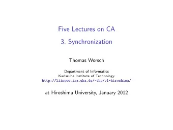
GLSVLSI 2007 17th edition of ACM Great Lakes Symposium on VLSI Design of Mixed Gates for Design of Mixed Gates for Leakage Reduction Leakage Reduction Frank Sill, Jiaxi You, Dirk Timmermann Institute of Applied Microelectronics and Computer
GLSVLSI 2007 17th edition of ACM Great Lakes Symposium on VLSI Design of Mixed Gates for Design of Mixed Gates for Leakage Reduction Leakage Reduction Frank Sill, Jiaxi You, Dirk Timmermann Institute of Applied Microelectronics and Computer Engineering University of Rostock, Germany 1 University of Rostock Institute of Applied Microelectronics and Computer Engineering Mixed Gates, Sill (GLSVLSI‘07)
Focus of this Work Focus of this Work 1. Advancement of established Leakage Reduction techniques (DVTCMOS / DTOCMOS) 2. Investigations on rules for Mixed Gates design DVTCMOS: Dual V th CMOS DTOCMOS: Dual T ox CMOS 2 University of Rostock Institute of Applied Microelectronics and Computer Engineering Mixed Gates, Sill (GLSVLSI‘07)
Outline Outline 1. Motivation 2. Basics 3. Mixed Gates 4. Design Rules 5. Benchmark results 6. Conclusions 3 University of Rostock Institute of Applied Microelectronics and Computer Engineering Mixed Gates, Sill (GLSVLSI‘07)
Motivation Motivation S. Borkar, ‘05 4 University of Rostock Institute of Applied Microelectronics and Computer Engineering Mixed Gates, Sill (GLSVLSI‘07)
Motivation Motivation Up to 50 % will be ( is ! ) leakage! SiO2 Lkg - Gate Oxide Tunneling Leakage ( I gate ) SD Lkg - Subthreshold Leakage ( I sub ) S. Borkar, ‘05 5 University of Rostock Institute of Applied Microelectronics and Computer Engineering Mixed Gates, Sill (GLSVLSI‘07)
2. Basics 2. Basics 6 University of Rostock Institute of Applied Microelectronics and Computer Engineering Mixed Gates, Sill (GLSVLSI‘07)
Power Dissipation in CMOS Power Dissipation in CMOS Gate I gate VDD Source Drain I gate SiO 2 I sub n + n + I dyn I sc I sub p - well L C L - I sub occurs if V gs < V th - carriers move by diffusion along surface GND - I gate caused by direct tunneling through gate oxide 7 University of Rostock Institute of Applied Microelectronics and Computer Engineering Mixed Gates, Sill (GLSVLSI‘07)
V th vs. Delay and Leakage V th vs. Delay and Leakage Inverter (BPTM 65 nm) 160 n 55 p Delay Subthreshold 50 p Leakage [A] 120 n Delay [s] Leakage 45 p 80 n 40 p 40 n 35 p 0 n 30 p 250 m 270 m 290 m 310 m 330 m 350 m 370 m Threshold Voltage Vth NMOS [V] 8 University of Rostock Institute of Applied Microelectronics and Computer Engineering Mixed Gates, Sill (GLSVLSI‘07)
V th vs. Delay and Leakage V th vs. Delay and Leakage Inverter (BPTM 65 nm) 160 n 55 p Subthreshold fast devices with high power dissipation (low V th ) Delay 50 p Leakage [A] 120 n Leakage Delay [s] or 45 p 80 n 40 p slow devices with low power dissipation (high V th ) 40 n 35 p 0 n 30 p 250 m 270 m 290 m 310 m 330 m 350 m 370 m Threshold Voltage Vth NMOS [V] 9 University of Rostock Institute of Applied Microelectronics and Computer Engineering Mixed Gates, Sill (GLSVLSI‘07)
T ox vs. Delay and Leakage T ox vs. Delay and Leakage Inverter (BPTM 65 nm) 160 n 50 p Gate- Delay Leakage [A] 45 p 120 n Delay [s] Leakage 40 p 80 n 35 p 40 n 30 p 0 n 25 p 14 16 17 18 20 22 Thickness of gate oxide (Tox) [10 -10 m] 10 University of Rostock Institute of Applied Microelectronics and Computer Engineering Mixed Gates, Sill (GLSVLSI‘07)
T ox vs. Delay and Leakage T ox vs. Delay and Leakage Inverter (BPTM 65 nm) 160 n 50 p fast devices with high power dissipation (low T ox ) Gate- Delay Leakage [A] 45 p 120 n Delay [s] Leakage 40 p or 80 n 35 p slow devices with low power dissipation (high T ox ) 40 n 30 p 0 n 25 p 14 16 17 18 20 22 Thickness of gate oxide (Tox) [10 -10 m] 11 University of Rostock Institute of Applied Microelectronics and Computer Engineering Mixed Gates, Sill (GLSVLSI‘07)
DVTCMOS / DTOCMOS DVTCMOS / DTOCMOS Dual Threshold Voltages (DVTCMOS) • Use different V th ’s – use lower threshold for devices within the critical paths – use higher threshold for devices outside the critical paths Dual Tox (DTOCMOS) • Use different T ox ’s – use thinner gate oxide for devices within the critical paths – use thicker gate oxide for devices outside the critical paths Decrease leakage without performance penalty 12 University of Rostock Institute of Applied Microelectronics and Computer Engineering Mixed Gates, Sill (GLSVLSI‘07)
DVTCMOS / DTOCMOS cont’ ’d d DVTCMOS / DTOCMOS cont critical path LVTO (low V th / T ox = fast, high leakage) HVTO (high V th / T ox = slow, low leakage) 13 University of Rostock Institute of Applied Microelectronics and Computer Engineering Mixed Gates, Sill (GLSVLSI‘07)
3. Mixed Gates 3. Mixed Gates 14 University of Rostock Institute of Applied Microelectronics and Computer Engineering Mixed Gates, Sill (GLSVLSI‘07)
Mixed- -V V th /T ox Pull- - Down/Up -Paths Paths Down/Up - Mixed th /T ox Pull Goal (for fast gates) : Preserve the delay while decreasing the leakage VDD 0 → 1 delay R (Output from GND to VDD) IN1 OUT IN2 1 → 0 delay (Output from VDD to GND) 2R delay 0 → 1 < delay 1 → 0 GND But : At timing analysis → only maximum delay is considered! 15 University of Rostock Institute of Applied Microelectronics and Computer Engineering Mixed Gates, Sill (GLSVLSI‘07)
Mixed- -V V th /T ox Pull- - Down/Up Down/Up - -Paths Cont Paths Cont’ ’d d Mixed th /T ox Pull Idea: Use different V th / T ox devices within a gate to adapt the delays High - Vth/Tox delay 0 → 1 = delay 1 → 0 Low - Vth/Tox 16 University of Rostock Institute of Applied Microelectronics and Computer Engineering Mixed Gates, Sill (GLSVLSI‘07)
Mixed Gates Mixed Gates Goal: Additional gate types at constant mask count Only two gate types in DVTCMOS / DTOCMOS → Problem: More high leakage gates after optimization as needed to keep the delay High - Vth/Tox Idea: Mixed V th / T ox gates to increase the amount of possible gate types Low - Vth/Tox 17 University of Rostock Institute of Applied Microelectronics and Computer Engineering Mixed Gates, Sill (GLSVLSI‘07)
Mixed Gates - - NAND2 NAND2 Mixed Gates Low - Vth/Tox High - Vth/Tox LVTO gate F - MG gate MG gate HVTO gate - rise time is shorter - rise and fall time are - middle delay cell - maximum delay cell than fall time nearly the same - middle leakage - minimum leakage - minimum delay cell - minimum delay cell - very high leakage - high leakage 18 University of Rostock Institute of Applied Microelectronics and Computer Engineering Mixed Gates, Sill (GLSVLSI‘07)
4. Design Rules 4. Design Rules 19 University of Rostock Institute of Applied Microelectronics and Computer Engineering Mixed Gates, Sill (GLSVLSI‘07)
Design Rules – – Why? Why? Design Rules - With two different device types: @2 input gate: at least 2 4 = 16 possibilities @3 input gate: at least 2 6 = 64 possibilities Design rules decrease library design time - Behavior of mixed stacks? 20 University of Rostock Institute of Applied Microelectronics and Computer Engineering Mixed Gates, Sill (GLSVLSI‘07)
Delay in Mixed Stacks Delay in Mixed Stacks - Two worst case scenarios: - Multi signal switch (MSS): all inputs switch together - Single signal switch (SSS): only lowest signal switches - Plateau-Phase [1]: - Internal voltages and current are constant - Dominates delay [1] Bisdounis et al., Analytical Transient Response and Propagation Delay Evaluation of the CMOS Inverter for Short-channel Devices", In IEEE Journal of Solid-State Circuits, 33-2, 1998. 21 University of Rostock Institute of Applied Microelectronics and Computer Engineering Mixed Gates, Sill (GLSVLSI‘07)
Multi Signal Switch Multi Signal Switch VDD V DD Out V in V out @MSS C L T top V int I stack Plateau Phase V pl V int @MSS T bottom 0 time - Plateau voltage V pl depends on top transistor T top in stack (only T top is saturated) - V pl determines current I stack through stack T top has highest influence on delay @MMS 22 University of Rostock Institute of Applied Microelectronics and Computer Engineering Mixed Gates, Sill (GLSVLSI‘07)
Single Signal Switch Single Signal Switch VDD V DD V in V int @SSS Out C L T top internal V out @SSS capacitances V int I stack discharges V pl Pleatau-Phase T bottom C int I discharge 0 time - In start phase: internal voltages have to discharged - T bottom has highest influence on I discarge T top and T bottom have highest influence on delay @SSS 23 University of Rostock Institute of Applied Microelectronics and Computer Engineering Mixed Gates, Sill (GLSVLSI‘07)
Leakage in Mixed Stack Leakage in Mixed Stack Subthreshold leakage I sub - I sub depends on input vector (stack effect) BUT : Positions of off-elements doesn’t matter Average I sub is depends only on amount of high-Vth/Tox elements Gate oxide leakage I gate - T bottom connected with GND T bottom has highest average gate leakage I gate 24 University of Rostock Institute of Applied Microelectronics and Computer Engineering Mixed Gates, Sill (GLSVLSI‘07)
Design Rules for Mixed Stacks Design Rules for Mixed Stacks Delay rule 1: If longest delay at MSS, then low-Vth/Tox as high as possible Delay rule 2: If longest delay at SSS, then at first T bottom then T top is low-Vth/Tox Leakage rule: Lowest possible transistor is high-Vth/Tox Rules are applied at design phase, until desired delay is reached. 25 University of Rostock Institute of Applied Microelectronics and Computer Engineering Mixed Gates, Sill (GLSVLSI‘07)
Recommend
More recommend
Explore More Topics
Stay informed with curated content and fresh updates.
