CSCI 510/610: Advanced Computer Architecture Implementing a Datapath - PDF document
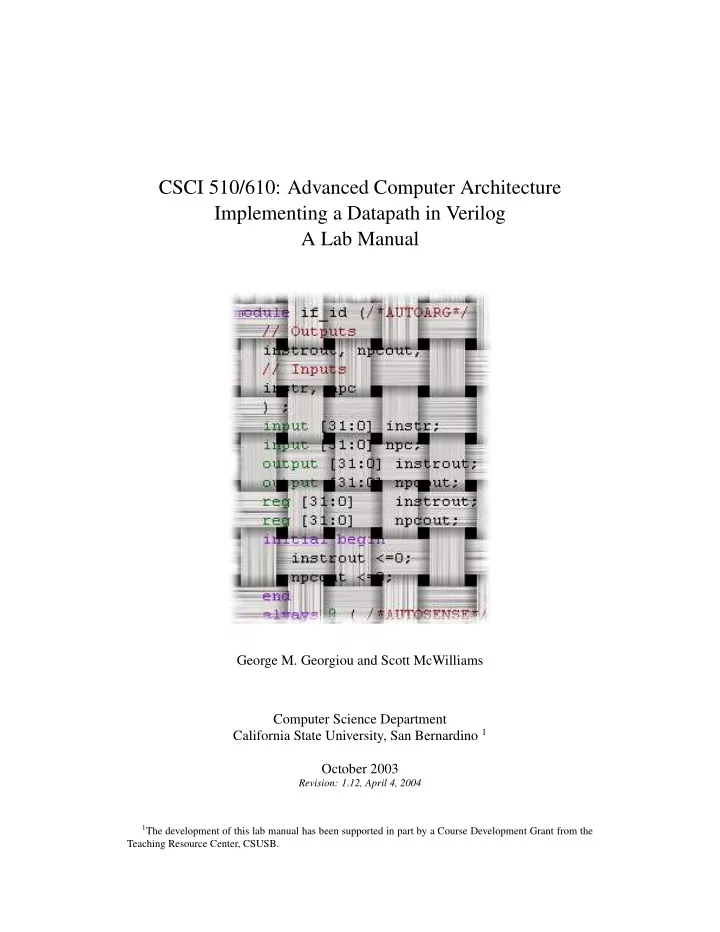
CSCI 510/610: Advanced Computer Architecture Implementing a Datapath in Verilog A Lab Manual George M. Georgiou and Scott McWilliams Computer Science Department California State University, San Bernardino 1 October 2003 Revision: 1.12, April
CSCI 510/610: Advanced Computer Architecture Implementing a Datapath in Verilog A Lab Manual George M. Georgiou and Scott McWilliams Computer Science Department California State University, San Bernardino 1 October 2003 Revision: 1.12, April 4, 2004 1 The development of this lab manual has been supported in part by a Course Development Grant from the Teaching Resource Center, CSUSB.
Contents Contents 1 List of Code Listings 2 List of Figures 3 I Lab Manual 5 1 The MIPS datapath in Verilog: The IF stage Lab 1–1 1.1 Testbenches . . . . . . . . . . . . . . . . . . . . . . . . . . . . . . . . . . . . . . Lab 1–5 2 The ID pipeline stage. Lab 2–1 3 The EX pipeline stage Lab 3–1 3.1 Testbenches . . . . . . . . . . . . . . . . . . . . . . . . . . . . . . . . . . . . . . Lab 3–5 4 The MEM pipeline stage. Lab 4–1 5 The WB pipeline stage Lab 5–1 6 Testing the MIPS datapath Lab 6–1 Bibliography Bib 1 1
List of Code Listings 1.1 Verilog code for the multiplexer. . . . . . . . . . . . . . . . . . . . . . . . . . . . Lab 1–3 1.2 The testbench for the multiplexor in figure 1.5 on page Lab 1–4 . . . . . . . . . . . Lab 1–6 1.3 The testbench for the incrementer in figure 1.6 on page Lab 1–4 . . . . . . . . . . Lab 1–7 3.1 The testbench for the 5-bit multiplexor in figure 3.3 on page Lab 3–3 . . . . . . . . Lab 3–6 3.2 The testbench for the ALU control in figure 3.4 on page Lab 3–4 . . . . . . . . . . Lab 3–7 3.3 The testbench for the ALU in figure 3.5 on page Lab 3–4 . . . . . . . . . . . . . . Lab 3–9 6.1 Binary code for testing the MIPS datapath. . . . . . . . . . . . . . . . . . . . . . . Lab 6–2 6.2 Initial data for memory. . . . . . . . . . . . . . . . . . . . . . . . . . . . . . . . . Lab 6–2 2
List of Figures 1.1 The revised MIPS datapath . . . . . . . . . . . . . . . . . . . . . . . . . . . . . . Lab 1–2 1.2 The IF stage . . . . . . . . . . . . . . . . . . . . . . . . . . . . . . . . . . . . . . Lab 1–2 1.3 The program counter (PC) . . . . . . . . . . . . . . . . . . . . . . . . . . . . . . Lab 1–3 1.4 The instruction memory . . . . . . . . . . . . . . . . . . . . . . . . . . . . . . . . Lab 1–3 1.5 The multiplexer . . . . . . . . . . . . . . . . . . . . . . . . . . . . . . . . . . . . Lab 1–4 1.6 The incrementer by 1 . . . . . . . . . . . . . . . . . . . . . . . . . . . . . . . . . Lab 1–4 1.7 The IF/ID pipeline register (latch) . . . . . . . . . . . . . . . . . . . . . . . . . . Lab 1–4 1.8 The output when running the testbench for the multiplexer (listing 1.2 on page Lab 1–6) . . . . . . . . . . . . . . . . . . . . . . . . . . . . . . . . . . . . . . . . . . Lab 1–5 1.9 The output when running the testbench for the incrementer (listing 1.3 on page Lab 1–7) . . . . . . . . . . . . . . . . . . . . . . . . . . . . . . . . . . . . . . . . . . Lab 1–5 2.1 The ID stage . . . . . . . . . . . . . . . . . . . . . . . . . . . . . . . . . . . . . . Lab 2–2 2.2 ALUOp Control Bit and Function Code Sets (after [4]) . . . . . . . . . . . . . . . Lab 2–2 2.3 The sign-extend unit . . . . . . . . . . . . . . . . . . . . . . . . . . . . . . . . . Lab 2–3 2.4 The control unit . . . . . . . . . . . . . . . . . . . . . . . . . . . . . . . . . . . . Lab 2–3 2.5 The register file . . . . . . . . . . . . . . . . . . . . . . . . . . . . . . . . . . . . Lab 2–4 2.6 The ID/EX pipeline register (latch) . . . . . . . . . . . . . . . . . . . . . . . . . . Lab 2–4 3.1 The EX stage . . . . . . . . . . . . . . . . . . . . . . . . . . . . . . . . . . . . . Lab 3–2 3.2 ALUOp Control Bit and Function Code Sets (after [4]) . . . . . . . . . . . . . . . Lab 3–2 3.3 The multiplexer . . . . . . . . . . . . . . . . . . . . . . . . . . . . . . . . . . . . Lab 3–3 3.4 The ALU control unit . . . . . . . . . . . . . . . . . . . . . . . . . . . . . . . . . Lab 3–4 3.5 The ALU . . . . . . . . . . . . . . . . . . . . . . . . . . . . . . . . . . . . . . . Lab 3–4 3.6 The adder . . . . . . . . . . . . . . . . . . . . . . . . . . . . . . . . . . . . . . . Lab 3–4 3.7 The EX/MEM pipeline register (latch) . . . . . . . . . . . . . . . . . . . . . . . . Lab 3–5 3.8 The output when running the testbench for the 5-bit multiplexer (listing 3.1 on page Lab 3–6) . . . . . . . . . . . . . . . . . . . . . . . . . . . . . . . . . . . . . Lab 3–5 3.9 The output when running the testbench for the ALU control (listing 3.2 on page Lab 3–7) . . . . . . . . . . . . . . . . . . . . . . . . . . . . . . . . . . . . . . . . . . Lab 3–8 3.10 The output when running the testbench for the ALU (listing 3.3 on page Lab 3–9) . Lab 3–8 4.1 The MEM stage . . . . . . . . . . . . . . . . . . . . . . . . . . . . . . . . . . . . Lab 4–2 4.2 The and gate . . . . . . . . . . . . . . . . . . . . . . . . . . . . . . . . . . . . . . Lab 4–2 4.3 The data memory unit . . . . . . . . . . . . . . . . . . . . . . . . . . . . . . . . . Lab 4–3 4.4 The MEM/WB pipeline register (latch) . . . . . . . . . . . . . . . . . . . . . . . . Lab 4–3 3
LIST OF FIGURES LIST OF FIGURES 5.1 The WB stage . . . . . . . . . . . . . . . . . . . . . . . . . . . . . . . . . . . . . Lab 5–1 5.2 The multiplexer . . . . . . . . . . . . . . . . . . . . . . . . . . . . . . . . . . . . Lab 5–2 4
Part I Lab Manual 5
LAB 1 The MIPS datapath in Verilog: The IF stage Objective: To implement and test the Instruction Fetch (IF) pipeline stage of the MIPS five stage pipeline. The series of labs in this manual has ultimate objective to implement and simulate in Verilog the MIPS pipeline datapath Figure 6.30 in Paterson and Hennessy’s textbook [4]. The model will be structural (as opposed to behavioral), but with one exception: basic units, such as multiplexors and ALU’s, may implemented as behavioral models. This approach reinforces the object-oriented style of programming, while at the same time relieving from the burden of structurally defining the basic units, which can be quite tedious, time consuming, and beyond the scope of this lab series. The slightly revised MIPS datapath to be implemented is in figure 1.1 on page Lab 1–2. For this week, you will implement the IF stage and test the fetching of instructions from memory. The IF stage isolated from the rest of the datapath can be seen in figure 1.2 on page Lab 1–2. • The names of the pipeline registers are IF ID, ID EX, EX MEM, MEM WB. For now, you will need only IF ID and EX MEM. • The instruction memory has 128 32-bit words. Later it will be expanded. All instructions and the PC are 32-bit wide. (Simply the 7 least significant bits (2ˆ7 = 128) are used for the time being.) • Implement the instruction memory, 2x1 MUX, and Incrementer-by-4 as separate modules. For the time being consider that the 1-bit signal PCSrc comes from a 1-bit register, PC choose. • Initialize IF ID IR (The instruction field of IF/ID) to 32 zeros. • Initialize IF ID NPC to 32 zeros. Initialize PC choose and EX MEM NPC to zeros. They will not change during this simulation. Initialize the first 10 words of memory (with addresses 0, 4, 8, etc.) with the following HEX values: Lab 1–1
LAB 1 The MIPS datapath in Verilog: The IF stage PCSrc� ID/EX� 2� \� WB� EX/MEM� IR�[31:26]� 0� 3� \� WB� x� M� WB� Control� MEM/WB� u� M� 4� \� EX� M� WB� 1� IF/ID� Add� Add� e� result� 1� t� i� Branch� W�r� Add� R�e�g� c� r� U�S� A�L� IR� [25:21]� e� t� i� Read reg 1� m�W�r� R�e�g� Read data 1� IR� Zero� e� o� [20:16]� M� m�t� PC� ALU� Address� Read reg 2� M�e� 0� IR� Instruction� ALU result� Address� Registers� x� memory� u� M� Read data� 1� Write reg� 1� Data� x� Read data 2� u� M� memory� Write data� 0� Write data� a�d� m�R�e� IR� IR� 16� 32� 6� M�e� [15:0]� [5:0]� ALU� Sign� \� \� \� control� extend� IR� ALUOp� 0� [20:16]� x� u� IR� M� [15:11]� 1� RegDst� Figure 1.1: The revised MIPS datapath PCSrc� From EX/MEM latch� 0� x� Component 1� u� M� 1� IF/ID� Add� Component 2� To ID/EX latch� 1� PC� Address� Component 3� Instruction� IR� memory� Component 4� Component 5� Figure 1.2: The IF stage Lab 1–2
LAB 1 The MIPS datapath in Verilog: The IF stage module mux ( a , b , s e l , y ) ; i n p u t [ 3 1 : 0 ] a , b ; i n p u t s e l ; output [ 3 1 : 0 ] y ; a s s i g n y = s e l ? a : b ; endmodule Listing 1.1: Verilog code for the multiplexer. A00000AA 10000011 20000022 30000033 40000044 50000055 60000066 70000077 80000088 90000099 • Turn in the source code and the printout of the clock cycle number, the contents of the PC (in decimal), IF ID IR (in hex), and IF ID NPC (in decimal) for 10 cycles of simulation. Be ready to demonstrate. Note: The code in listing 1.1 implements the multiplexer in the IF stage as a combinational circuit. 32� 32� npc� PC� \� \� PC� Figure 1.3: The program counter (PC) 32� addr� Address� \� Instruction� 32� data� \� memory� Figure 1.4: The instruction memory Lab 1–3
Recommend


More recommend
Explore More Topics
Stay informed with curated content and fresh updates.