Continuous Time Sigma Delta Modulators and VCO ADCs Pieter Rombouts - PowerPoint PPT Presentation
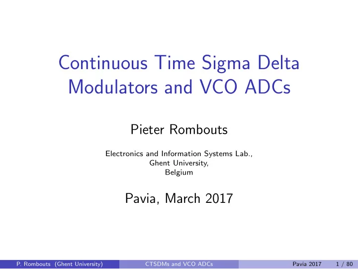
Continuous Time Sigma Delta Modulators and VCO ADCs Pieter Rombouts Electronics and Information Systems Lab., Ghent University, Belgium Pavia, March 2017 P. Rombouts (Ghent University) CTSDMs and VCO ADCs Pavia 2017 1 / 80 Outline Sigma
Continuous Time Sigma Delta Modulators and VCO ADCs Pieter Rombouts Electronics and Information Systems Lab., Ghent University, Belgium Pavia, March 2017 P. Rombouts (Ghent University) CTSDMs and VCO ADCs Pavia 2017 1 / 80
Outline Sigma Delta Modulation 1 Continuous Time Sigma Delta Modulation 2 FoM Confusion 3 VCO ADC 4 Conclusion 5 P. Rombouts (Ghent University) CTSDMs and VCO ADCs Pavia 2017 2 / 80
A/D converter: traditional interpretation U I converts analog value into digital number of bits n ◮ quantisation step q: q = V ref / 2 n error within ± q / 2 staircase I/O ◮ static nonlinearity ◮ INL or DNL P. Rombouts (Ghent University) CTSDMs and VCO ADCs Pavia 2017 3 / 80
A/D converter: other interpretation Q U I U I converts analog signal into digital signal quantisation eror Q ◮ (white) noise signal ◮ like other noise contributions ◮ number of bits not essential ⋆ large enough Leave margin for other noise sources ⋆ effective bits quantisation noise variance Q = q 2 σ 2 12 P. Rombouts (Ghent University) CTSDMs and VCO ADCs Pavia 2017 4 / 80
Core concept 1: Oversampling signal spectrum spectrum white noise 0.1 0.2 0.3 0.4 0.5 0.1 0.2 0.3 0.4 0.5 frequency/f sample frequency/f sample Oversampling ratio: OSR = f S 2 f 0 P. Rombouts (Ghent University) CTSDMs and VCO ADCs Pavia 2017 5 / 80
Core concept 1: Oversampling signal spectrum spectrum white noise 0.1 0.2 0.3 0.4 0.5 0.1 0.2 0.3 0.4 0.5 frequency/f sample frequency/f sample ideal digital filter after quantizer ◮ averaging mechanism ◮ number of bits has increased ◮ less noise ◮ filters signal as well ⋆ not Nyquist-rate anymore! P. Rombouts (Ghent University) CTSDMs and VCO ADCs Pavia 2017 6 / 80
Core concept 1: Oversampling signal spectrum spectrum white noise 0.1 0.2 0.3 0.4 0.5 0.1 0.2 0.3 0.4 0.5 frequency/f sample frequency/f sample quantisation noise variance q 2 1 σ 2 Q = 12 OSR ∼ OSR 3dB/octave improvement P. Rombouts (Ghent University) CTSDMs and VCO ADCs Pavia 2017 7 / 80
The Σ∆ control loop Q V in V in D D + + + H quant H � � � - - DAC (a) (b) ideal DAC filter ◮ discrete time ◮ continuous time P. Rombouts (Ghent University) CTSDMs and VCO ADCs Pavia 2017 8 / 80
The Σ∆ control loop Q V in V in D D + + + H quant H � � � - - DAC (a) (b) 1 H D = 1 + H V in + 1 + H Q for low frequencies H ≈ ∞ − → D ≈ V in nullator P. Rombouts (Ghent University) CTSDMs and VCO ADCs Pavia 2017 9 / 80
The Σ∆ control loop H 1 D = 1 + H V in + 1 + H Q � �� � error input signal is also filtered 1 for low frequencies NTF = 1+ H ≈ 0 1 for high frequencies NTF = 1+ H � = 0 P. Rombouts (Ghent University) CTSDMs and VCO ADCs Pavia 2017 10 / 80
Core concept 2: ”Noise” Shaping NTF(z) 1 freq. DC f sample /2 1 for high frequencies NTF = 1+ H � = 0 spectral shaping P. Rombouts (Ghent University) CTSDMs and VCO ADCs Pavia 2017 11 / 80
Core concept 2: “Noise” Shaping signal shaped noise freq. freq. DC DC f sample /2 f sample /2 (a) (b) noise spectrum has the shape of NTF combine with oversampling − → most noise vanishes P. Rombouts (Ghent University) CTSDMs and VCO ADCs Pavia 2017 12 / 80
Σ∆ Modulators Q V in V in D D + + + H quant H � � � - - DAC (a) (b) quantizer ◮ very few bits ◮ accuracy from oversampling + noise shaping ◮ 1 bit P. Rombouts (Ghent University) CTSDMs and VCO ADCs Pavia 2017 13 / 80
Σ∆ Modulators Q V in V in D D + + + H quant H � � � - - DAC (a) (b) 1-bit quantizer ◮ simple ◮ inherent linear ◮ noise is not white ⋆ tones ⋆ stability P. Rombouts (Ghent University) CTSDMs and VCO ADCs Pavia 2017 14 / 80
Σ∆ Modulators Q V in V in D D + + + H quant H � � � - - DAC (a) (b) multi-bit quantizer ◮ better performance ◮ DAC needs linearization ⋆ DEM ⋆ calibration ◮ always larger area P. Rombouts (Ghent University) CTSDMs and VCO ADCs Pavia 2017 15 / 80
Σ∆ Modulators Q V in V in D D + + + H quant H � � � - - DAC (a) (b) filter ◮ cascade of integrators ◮ order: design parameter ⋆ trade-off complexity-performance ◮ special design techniques ⋆ Richard Schreier’s toolbox P. Rombouts (Ghent University) CTSDMs and VCO ADCs Pavia 2017 16 / 80
1st order, 1bit Σ∆ Modulator Typical circuit C C V in - + b i V ref + b i D Q - clk switched cap devices can be very small ◮ also C ◮ (thermal) noise ↓ due to oversampling P. Rombouts (Ghent University) CTSDMs and VCO ADCs Pavia 2017 17 / 80
High Order Σ∆ Modulators Cascade of integrators with feedback u ( n ) b 1 b 2 b 3 b 4 -g 1 x 1 ( n ) x 2 ( n x 3 ( n ) y ( n ) 1 1 1 c 1 c 2 c 3 v ( n ) z -1 z -1 z -1 -a 1 -a 2 -a 3 DAC without extra feed ins ◮ high swing on internal nodes ◮ ‘poor’ distortion performance P. Rombouts (Ghent University) CTSDMs and VCO ADCs Pavia 2017 18 / 80
High Order Σ∆ Modulators Cascade of integrators with feedforward u ( n ) b 1 b 2 b 3 b 4 -g 1 x 1 ( n ) x 2 ( n x 3 ( n ) y ( n ) 1 1 1 c 2 c 3 a 3 v ( n ) z -1 z -1 z -1 a 2 -c 1 a 1 DAC without extra feed ins ◮ negligible swing on internal nodes ◮ excellent distortion performance P. Rombouts (Ghent University) CTSDMs and VCO ADCs Pavia 2017 19 / 80
Σ∆ ADC analog digital f < f f = f cuto ff cuto ff 0 S f S 2f 0 D out V in anti-aliasing Sigma Delta lowpass pre fi lter modulator fi lter decimation fi lter several filters in chain ◮ simple anti-aliasing filter ◮ no sample-to-sample correspondence number of bits in D out high enough P. Rombouts (Ghent University) CTSDMs and VCO ADCs Pavia 2017 20 / 80
Σ∆ ADC analog digital f < f f = f cuto ff cuto ff 0 S f S 2f 0 D out V in anti-aliasing Sigma Delta lowpass pre fi lter modulator fi lter decimation fi lter scientific literature ◮ without filters ◮ accuracy calculated from ideal filter P. Rombouts (Ghent University) CTSDMs and VCO ADCs Pavia 2017 21 / 80
OSR Low OSR? ◮ keep f s feasable ◮ need many quantizer bits ◮ need high order filter ◮ minimum 8 High OSR? ◮ small devices ⋆ noise is filtered ◮ low filter order ◮ 1-bit quantiser P. Rombouts (Ghent University) CTSDMs and VCO ADCs Pavia 2017 22 / 80
Outline Sigma Delta Modulation 1 Continuous Time Sigma Delta Modulation 2 FoM Confusion 3 VCO ADC 4 Conclusion 5 P. Rombouts (Ghent University) CTSDMs and VCO ADCs Pavia 2017 23 / 80
CTSDM vs DTSDM Σ∆ modulators ◮ oversampling and noise shaping ◮ high-accuracy P. Rombouts (Ghent University) CTSDMs and VCO ADCs Pavia 2017 24 / 80
CTSDM vs DTSDM Discrete-time ◮ versatile ◮ “simple” design ◮ easy to “abuse” standard cell IP core Continuous-time ◮ potential for higher speed ◮ potential for lower power ◮ anti-aliasing ◮ non-trivial design (needs tuning) ◮ performance and stability depend on f clk ◮ common myth: sensitive to clock jitter P. Rombouts (Ghent University) CTSDMs and VCO ADCs Pavia 2017 25 / 80
Continuous Time Σ∆ modulator f s a 1 a N . . . quant Σ Σ Σ V in ( s ) D out ( z ) sT s sT s − − − . . . ZOH ( s ) ZOH ( s ) closed feedback loop ◮ cascade of integrators with feedback ◮ cascade of integrators with feedforward . . . loop filter = continuous time sampler inside loop P. Rombouts (Ghent University) CTSDMs and VCO ADCs Pavia 2017 26 / 80
Continuous Time Σ∆ modulator Linearized model Q f s a 1 a N . . . Σ Σ Σ V in ( s ) Σ D out ( z ) sT s sT s − − − . . . ZOH ( s ) ZOH ( s ) output contains two contributions ◮ Input signal ◮ Quantisation noise superposition P. Rombouts (Ghent University) CTSDMs and VCO ADCs Pavia 2017 27 / 80
Quantization noise Q f s a N a 1 ... Σ Σ Σ Σ D out (z) sT s sT s − − − ... ZOH(s) ZOH(s) Q Σ D out (z) − f s H(s) ZOH(s) H eq (z) equivalent discrete time loop filter H eq ( z ) ◮ fully equivalent ◮ impulse invariant transform of H ( s ) ◮ CT - DT relationship: z = e sT clk P. Rombouts (Ghent University) CTSDMs and VCO ADCs Pavia 2017 28 / 80
Quantization noise Q Σ D out (z) − f s H(s) ZOH(s) H eq (z) 1 H eq + 1 · Q = NTF · Q equivalent to DT Σ∆ modulator P. Rombouts (Ghent University) CTSDMs and VCO ADCs Pavia 2017 29 / 80
Quantization noise Q Σ D out (z) − f s H(s) ZOH(s) H eq (z) remarks ◮ theory = mature ⋆ e.g. c2d function in matlab ◮ H eq depends on Dac-pulse ◮ H eq depends on f s ◮ H eq sensitive to analog imperfections ⋆ ‘excess’ loop delay ⋆ parasitic (opamp) poles P. Rombouts (Ghent University) CTSDMs and VCO ADCs Pavia 2017 30 / 80
Continuous Time Σ∆ modulator Linearized model Q f s a 1 a N . . . Σ Σ Σ V in ( s ) Σ D out ( z ) sT s sT s − − − . . . ZOH ( s ) ZOH ( s ) output contains two contributions ◮ Input signal ◮ Quantisation noise superposition P. Rombouts (Ghent University) CTSDMs and VCO ADCs Pavia 2017 31 / 80
Input signal f s a 1 a N ... Σ Σ Σ V in (s) D out (z) sT s sT s − − − ... ZOH(s) ZOH(s) f s Σ V in (s) G(s) D out (z) − f s H(s) ZOH(s) H eq (z) P. Rombouts (Ghent University) CTSDMs and VCO ADCs Pavia 2017 32 / 80
Recommend
More recommend
Explore More Topics
Stay informed with curated content and fresh updates.
